BL702/704/706 Reference Manual
Name
Description
spi_fifo_config_0 SPI FIFO configuration register0
spi_fifo_config_1 SPI FIFO configuration register1
spi_fifo_wdata SPI FIFO write data
spi_fifo_rdata SPI FIFO read data
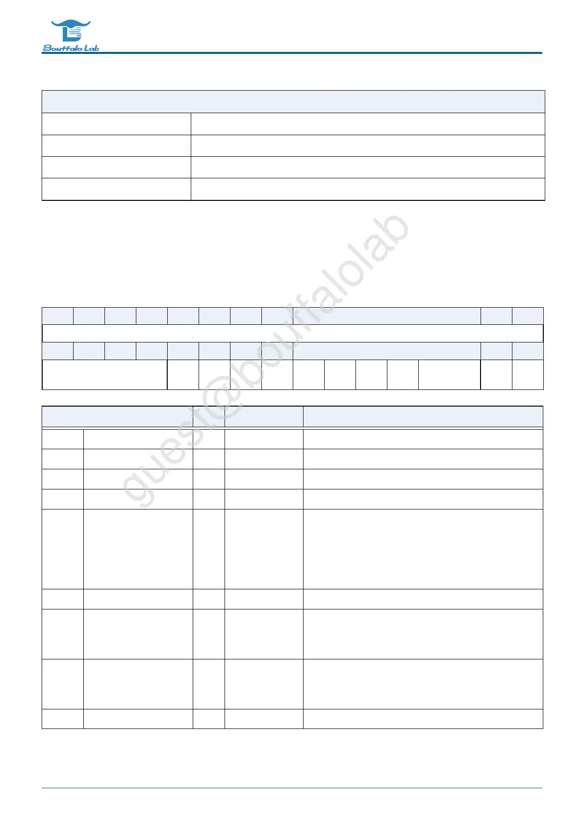
9.4.1 spi_config
Address:0x4000a200
31 30 29 28 27 26 25 24 23 22 21 20 19 18 17 16
RSVD
15 14 13 12 11 10 9 8 7 6 5 4 3 2 1 0
DEGCNT DEG
EN
RSVD MCEN IGNR
EN
BYTE
INV
BIT
INV
SCLK
PH
SCLK
POL
FSIZE SEN MEN
Bits
Name Type Reset Description
31:16 RSVD
15:12 DEGCNT R/W 4’d0 De-glitch function cycle count
11 DEGEN R/W 1’b0 Enable signal of all input de-glitch function
10 RSVD
9 MCEN R/W 1’b0 Enable signal of master continuous transfer mode
1’b0: Disabled, SS_n will de-assert between each data
frame
1’b1: Enabled, SS_n will stay asserted between each con-
secutive data frame if the next data is valid in the FIFO
8 IGNREN R/W 1’b0 Enable signal of RX data ignore function
7 BYTEINV R/W 1’b0 Byte-inverse signal for each FIFO entry data
0: Byte[0] is sent out first
1: Byte[3] is sent out first
6 BITINV R/W 1’b0 Bit-inverse signal for each data byte
0: Each byte is sent out MSB-first
1: Each byte is sent out LSB-first
5 SCLKPH R/W 1’b0 SCLK clock phase inverse signal
BL702/704/706 Reference Manual 182/ 375
@2021 Bouffalo Lab