10-17
PHYSICAL DESIGN AND SYSTEM DEBUGGING
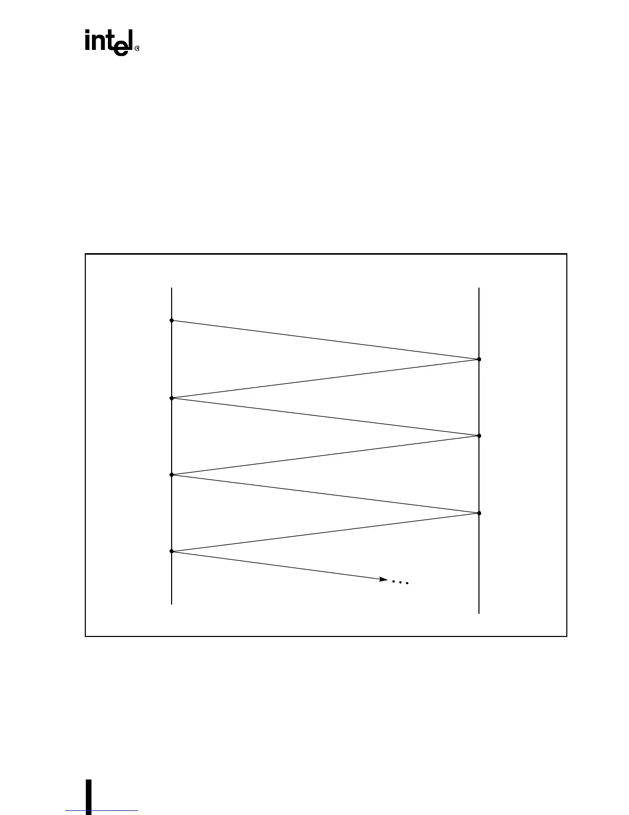
V
a
= V
S
· {75/(75+30)} = 2.64286 V
V
r1
= 2.64286 x 0.14286 = 0.37755 V
V
r2
= 0.37755 x –0.42875 = –0.16181 V
V
r3
= –0.16181 x 0.14286 = –0.02312 V
V
r4
= –0.02312 x –0.42857 = 0.00991 V
V
r5
= 0.00991 x 0.14286 = 0.00142 V
V
r6
= 0.00142 x –0.42857 = –0.00061 V
V
r7
= –0.00061 x 0.14286 = –0.00009 V
Figure 10-12 shows the corresponding lattice diagram.
Figure 10-12. Lattice Diagram Example
Impedance discontinuity problems are managed by imposing limits and control during the rout-
ing phase of the design. Design rules must be observed to control trace geometry, including spec-
ification of the trace width and spacing for each layer. This is very important because it ensures
the traces are smooth and constant without sharp turns.
5t
pd
2.847 V
3t
pd
2.835 V
t
pd
3.02 V
V(A,t) t = 0
2.857 V 2t
pd
2.845 V 4t
pd
2.846 V 6t
pd
V
r
6
=
0
.
0
0
0
6
1
V
A
=
2
.
6
4
V
r
1
=
0
.
3
7
8
V
r
3
=
-
0
.
0
2
3
1
V
r
5
=
0
.0
0
1
4
2
V
r
2
=
-
0
.
1
6
2
V
r
4
=
0
.
0
0
9
9
A B
V(B,t)
7t
pd
2.846 V