2FD/2FF/2FG
2-2-1
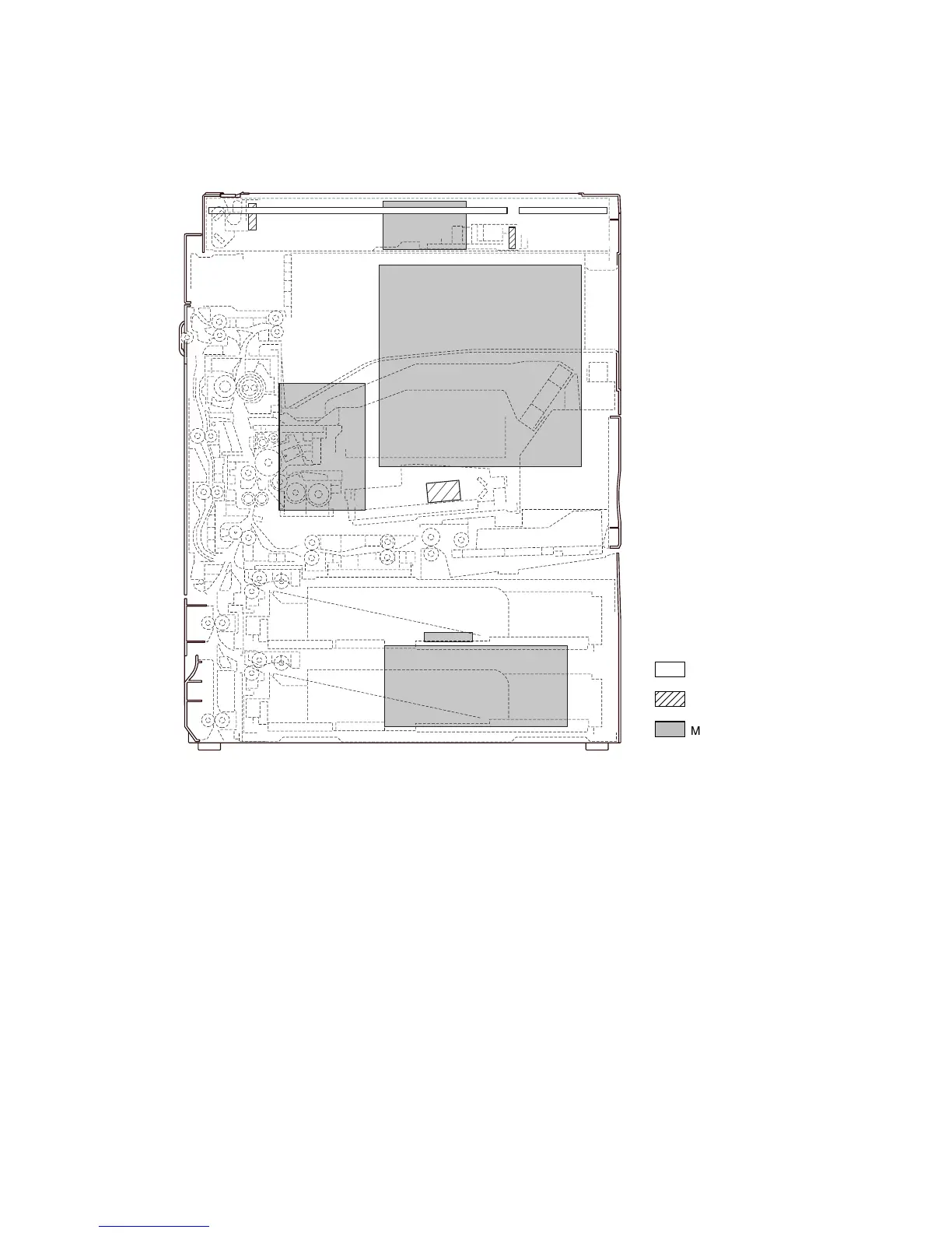
2-2-1 Electrical parts layout
(1) PCBs
Figure 2-2-1 PCBs
1. Main PCB (MPCB) ....................................... Controls the other PCBs, electrical components and optional devices.
2. Power source PCB (PSPCB) ....................... Generates +24 V DC, 12 V DC and 5V DC; controls the fixing heater.
3. High-voltage transformer PCB
(HVTPCB) .................................................... Main charging. Generates developing bias and high voltages for
transfer.
4. Scanner drive PCB (SDPCB) ...................... Controls the scanning section.
5. Inverter PCB (INPCB) .................................. Controls the exposure lamp.
6. CCD PCB (CCDPCB) .................................. Reads the image off originals.
7. Right operation unit PCB (OPCB-R) ............ Consists of the operation keys and display LEDs.
8. Left operation unit PCB (OPCB-L) ............... Controls touch panel and LCD indication.
9. Laser diode PCB (LDPCB) .......................... Generates and controls the laser light.
10. Noise filter PCB (NFPCB) ............................ Reducts the noise.
2
1
4
3
9
5
87
6
Machine front
Machine inside
 Loading...