2FD/2FF/2FG
2-3-25
2-3-5 CCD PCB
1
2
RS
CLP
SHIFT
Odd
Even
RS
CLK
CLP
Clock driver
IC1, 4
Differential
receiver
IC3
Main PCB
CCD PCB
CCD
IC2
Transistor Q2
Transistor Q1
SHIFT
Odd
Even
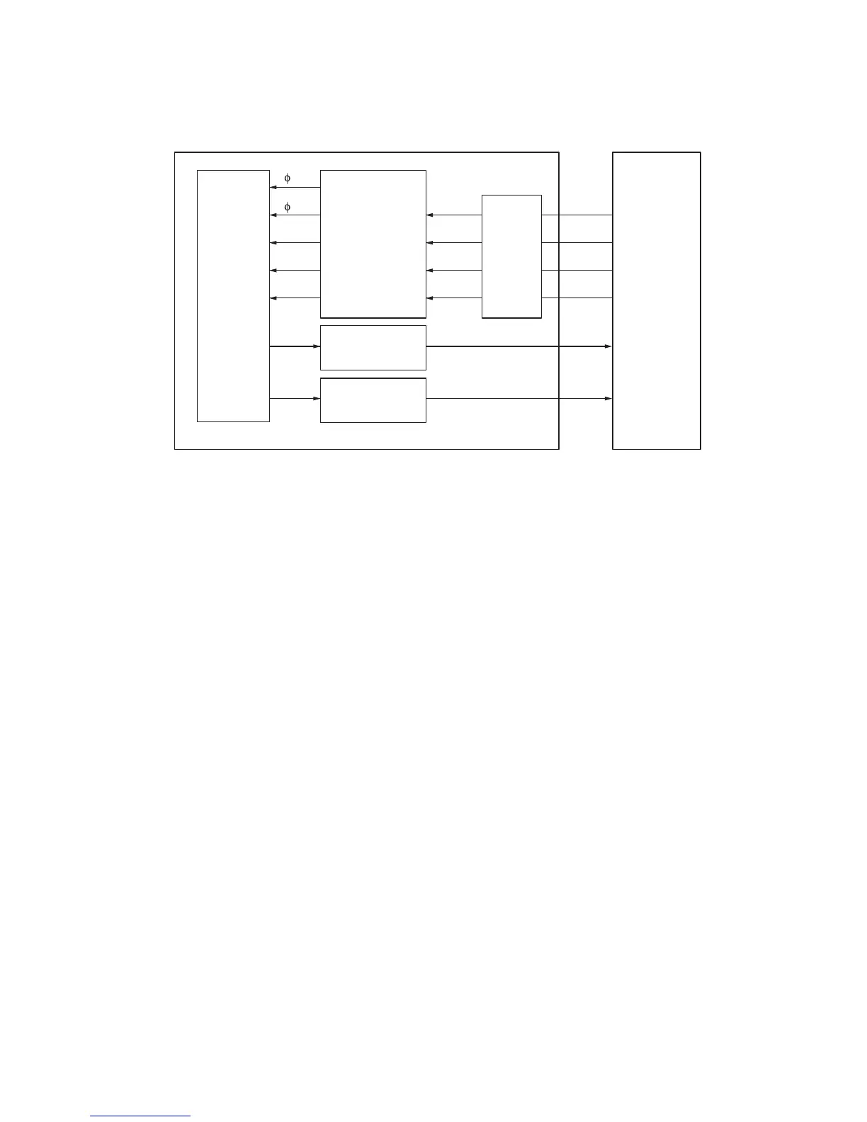
Figure 2-3-10 CCD PCB block diagram
The CCD PCB (CCDPCB) is equipped with a CCD sensor IC2 for original scanning.
The clock signals (CLK, RS, CLP, and SHIFT) for driving the CCD sensor (IC2) are sent as differential signals from the main
PCB (MPCB), reconstructed to normal signals by the differential receiver (IC3), and then input to the CCD sensor (IC2) via
the clock driver (IC1 and IC4).
Image signals are analog signals. Even- and odd-numbered pixels are output separately. These analog image signals are
amplified by emitter followers in the transistors Q1 and Q2 and then transmitted to the analog signal processing circuit in the
main PCB (MPCB).
 Loading...