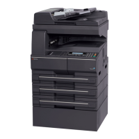
2KJ/2KH
2-3-4
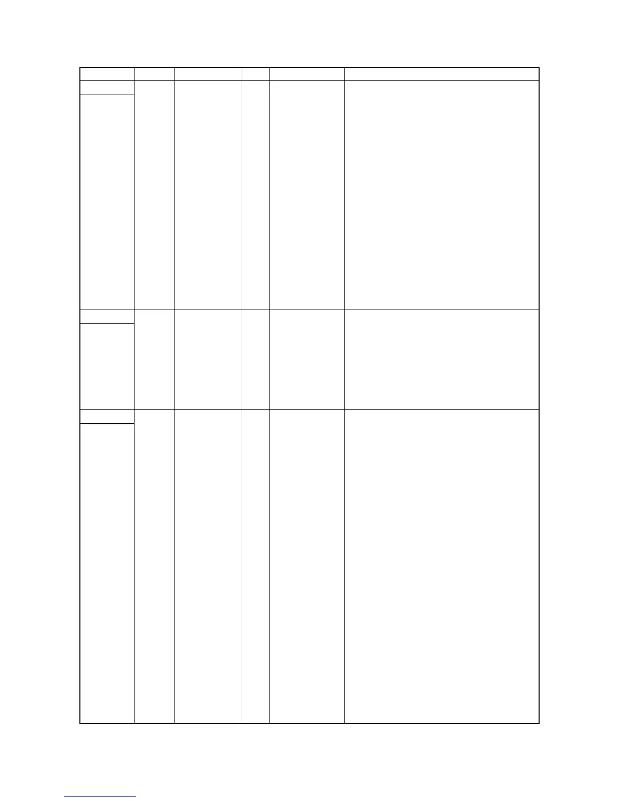
Connector Pin No. Signal I/O Voltage Description
YC5 1 5V O 5 V DC 5 V DC power output to CCDPWB
Connected
to the CCD
PWB
2 NC - - Not used
3 TG O 0/3.3 V DC CCD control signal
4 GND - - Ground
5 RS I 0/3.3 V DC CCD control signal
6 GND - - Ground
7 CP O 0/3.3 V DC CCD control signal
8 GND - - Ground
9 PHY2 - 0/3.3 V DC (pulse) CCD clock signal
10 GND - - Ground
11 GND - - Ground
12 Vout1 Analog CCD output signal
13 Vout2 Analog CCD output signal
14 GND - - Ground
15 NC - - Not used
16 CCDPWR O 12 V DC 12 V DC power output to CCDPWB
YC6 1 PDN I 0/3.3 V DC Laser sync signal
Connected
to the APC
PWB
2SGND -- Ground
3 OUTREN O 0/3.3 V DC Laser diode output signal
4 SAMPLEN O 0/3.3 V DC Sample hold signal
5 VDON O - Image data signal
6 VDOP O - Image data signal
7 5V1 O 5 V DC 5 V DC power output to APCPWB
YC7 1 _RST_ENG O 0/3.3 V DC EPWB reset signal
Connected
to the
engine PWB
2 SCANHLD O 0/3.3 V DC EPWB hold signal
3 ENGHLD O 0/3.3 V DC EPWB hold signal
4 AFEOVSYNC I 0/3.3 V DC (pulse) Image control signal
5 GND - - Ground
6 _24V_DOWN I 0/3.3 V DC EPWB 24 V down signal
7 PVSYNC I 0/3.3 V DC (pulse) Image control signal
8 GND - - Ground
9 EGOUTPEN I 0/3.3 V DC Laser diode output signal
10 PLGCLK O 0/3.3 V DC (pulse) PM clock signal
11 SLEEP O 0/3.3 V DC EPWB sleep signal
12 GND - - Ground
13 EGSIRN I 0/3.3 V DC EPWB interrupt signal
14 EGSDIR I 0/3.3 V DC EPWB communication direction signal
15 GND - - Ground
16 EGSBSY I 0/3.3 V DC EPWB busy signal
17 EGSDO_BUF O 0/3.3 V DC (pulse) EPWB serial communication data signal
18 GND - - Ground
19 EGSCLK_BUF O 0/3.3 V DC (pulse) EPWB clock signal
20 EGSDI I 0/3.3 V DC (pulse) EPWB serial communication data signal
 Loading...