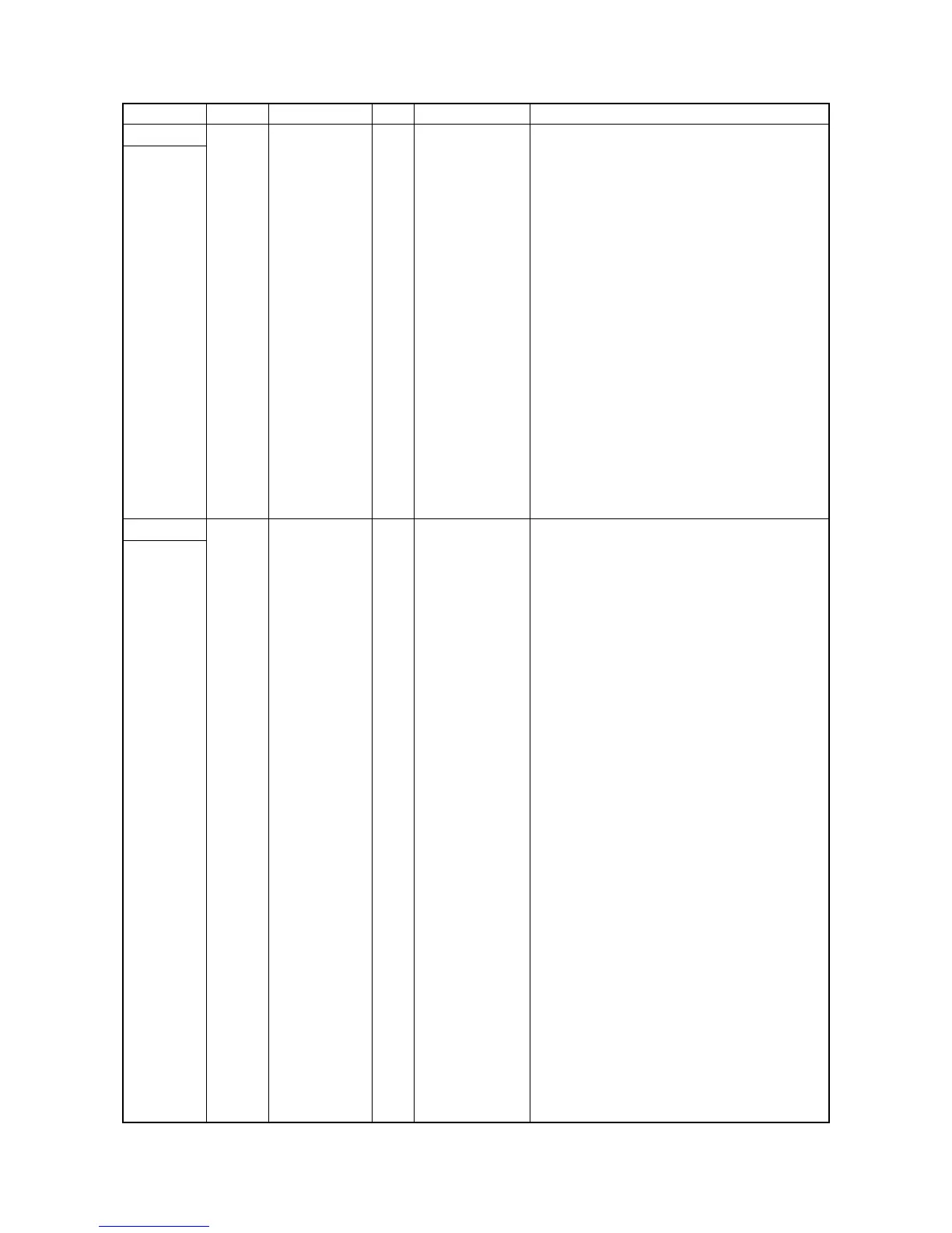
2KJ/2KH
2-3-9
YC4 1 RLSOLN O 0/24 V DC FSSOL: On/Off (return)
Connected
to the built-
in finisher or
job separa-
tor
2 SLSOLN O 0/24 V DC FSSOL: On/Off (activate)
3 UOPSCLK O 0/5 V DC (pulse) Built-in finisher/Job separator clock signal
4 UOPSDI I DC0V/5(þ?Ÿ¾) Built-in finisher serial communication data signal /
Job separator JBESW: On/Off
5 UOPSDO O 0/5 V DC (pulse) Built-in finisher/Job separator serial communica-
tion data signal
6 UOPSRDY I 0/5 V DC Built-in finisher ready signal /
Job separator EPDSW: On/Off
7 UOPSEL O 0/5 V DC Built-in finisher/Job separator select signal
8SGND -- Ground
9 +5V4 O 5 V DC 5 V DC power output to built-in finisher/Job sepa-
rator
10 PGND - - Ground
11 PGND - - Ground
12 +24V1 O 24 V DC 24 V DC power output to built-in finisher/Job sep-
arator
13 +24V1 O 24 V DC 24 V DC power output to built-in finisher/Job sep-
arator
YC5 A1 ORGTIMN I 0/5 V DC Original scanning interval signal
Connected
to the docu-
ment pro-
cessor,
original size
detection
sensor,
home posi-
tion sensor
and original
detection
switch
A2 DOPRDY I 0/5 V DC Document processor ready signal
A3 DOPSEL O 0/5 V DC Document processor select signal
A4 SGND - - Ground
A5 DOPCLK O 0/5 V DC (pulse) Document processor clock signal
A6 DOPSDI I 0/5 V DC (pulse) Document processor serial communication data
signal
A7 DOPSDO O 0/5 V DC (pulse) Document processor serial communication data
signal
A8 +5V4 O 5 V DC 5 V DC power output to document processor
A9 PGND - - Ground
A10 PGND - - Ground
A11 +24V1 O 24 V DC 24 V DC power output to document processor
A12 NC - - Not used
B1 +5V4 O 5 V DC 5 V DC power output to OSDS
B2 ORGLSWN I 0/3.3 V DC OSDS: On/Off
B3 SGND - - Ground
B4 +5V4 O 5 V DC 5 V DC power output to HPSW
B5 HPSWN I 0/3.3 V DC HPSW: On/Off
B6 SGND - - Ground
B7 +5V4 O 5 V DC 5 V DC power output to ODSW
B8 OPSWN I 0/3.3 V DC ODSW: On/Off
B9 SGND - - Ground
B10 NC - - Not used
B11 NC - - Not used
B12 NC - - Not used
Connector Pin No. Signal I/O Voltage Description
 Loading...