– 2.9 –
2-1-7. IO2 PCB
This board is a located in the instrumentation box. It receives various sensor signals and
transfers data to the main board. It mounts the exhaust fan, heater control circuit, and sleep
refresh control circuit.
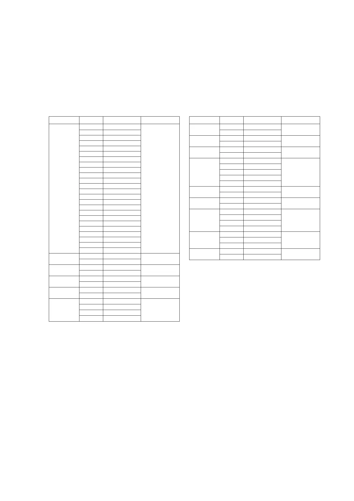
IO2 PCB Connector signals
Connector Pin No. Signal name Remarks
1 +35V
2 SPCK-02
3 +35V
4 SPLD-02
5 +35V
6Q2
7GATE
8 +35V
9 SPLD-02
10 +35V
11 SPCK-I2
12 +35V
13 SPDA-I2
14 GND
15 /ACS2
16 GND
17 ASCK2
18 GND
19 ADI2+
20 +5V
21 A4A2
22 A4B2
23 A4C2
24 +5V
1 +LED1 Orange LED
2 -LED1 (Print)
1 +LED2 Orange LED
2 -LED2 (Pri)
1 +LED3 Green LED
2 -LED3 (Print)
1 +LED4 Green LED
2 -LED4 (Pri)
1 +5V Heater switch
2 SW1
3 +5V
4 SW2
CN2
CN3
CN4
CN5
CN6
CN7
CN8
CN1
Attach FPC with
the terminal side
up (reinforcing
plate down) .
Connector Pin No. Signal name Remarks
1 SW1 SSR (Print)
2 SSR1
1 SW2 SSR (Pri)
2 SSR2
1+FAN Fan 1
2-FAN (Inside)
1+FAN Fan 2
2-FAN (Outside)
3-FAN
4-FAN
1 TH1 Thermisitor
2 GND (Print)
1 TH1 Thermisitor
2 GND (Pri)
1 +5VSB Remote switch
2SB
3 LED
4 GND
1 +5VSB
2 GND
3 P/S ON
1+FANFan relay PCB
2-FAN
CN12
CN13
CN14
CN15
CN22
CN23
CN25

 Loading...