Hardware Principle 4-5
4.2.2.1 Front-end of main board
Main board
HVISO
32ch
BF FPGA
Control
signal
DATA
DSP
FPGA
High-voltage control signal
IQ
DDR2
UPLOAD
DDR2
PCIE X1
CPLD control signal
Rx9~
16
Rx49~64
or
Tx25~32
Rx1~8
…
...
LVDS*8
Tx9~16
Tx49~64
or
Tx25~32
Tx1~8
Probe
board
PCIE
PHY
Communication
control bus
Control
signal
…
...
High-
voltage
pulse
output
circuit
Drive
circuit
Tx
TGC
8-channel digital
LNA VGA ADC
Rx
8-channel analog
Control signal
Control signal
CPU
module
Clock
circuit
Clock
Clock
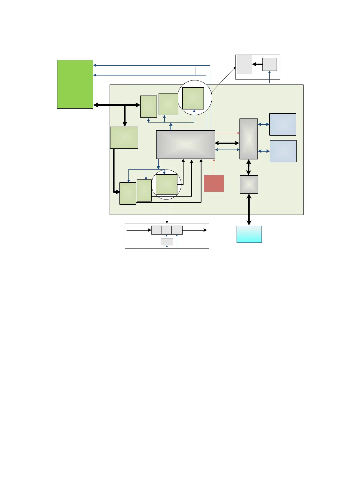
Figure 4-4 Principle Diagram of Front-end of the Main Board
As shown in the figure above, ultrasound front-end internal structure consists of ultrasound
receiving module(Rx1~Rx64), ultrasound transmission module(Tx1~Tx64), high-voltage isolation
module(HVISO), BF FPGA module, DSP FPGA module ,PCIE_PHY module and so on.
Ultrasound receiving module(Rx1~Rx32), ultrasound transmission module(Tx1~Tx32),
high-voltage isolation module(HVISO)of Z5 series are half of Z6 series.
Function describes as following:
Support 32/64-channel high-voltage isolation(HVISO)to protect ultrasound receiving
module(Rx)to avoid ultrasound transmission high-voltage contamination.
32/64-channel transmission wave forms according to scanning time sequence and control
parameters.
32/64-channel transmission wave forms to 32/64-channel high-voltage transmission wave
by driver.
Echo receiving LNA is to enlarge fixed gain.
By the control of TGC, echo receiving carries out variable gain amplification by depth.
32/64-channel analog echo could be switched to 32/64-channel digital signal by ADC.
BF FPGA combines 64-channel echo signal to output to DSP FPGA, and DSP FPGA is
sent to signal processing to a single image which is uploaded to CPU module by
PCIE_PHY, then CPU module performs post processing.
PCI_PHY implements PCIE interface switching.
BF FPGA can communicate with the CPU module through transferring DSP FPGA.
 Loading...