Hardware Principle 4-13
Back-end of main board (FPGA core voltage)
Front-end of main board (receiving chip)
Back-end of main board ( video encoder, FPGA IO voltage ,
DDR2)
Back-end of main board ( video encoder, FPGA IO voltage)
Probe board (high-voltage switch)
Probe board (high-voltage switch)
Transmitting high-voltage
Transmitting high-voltage
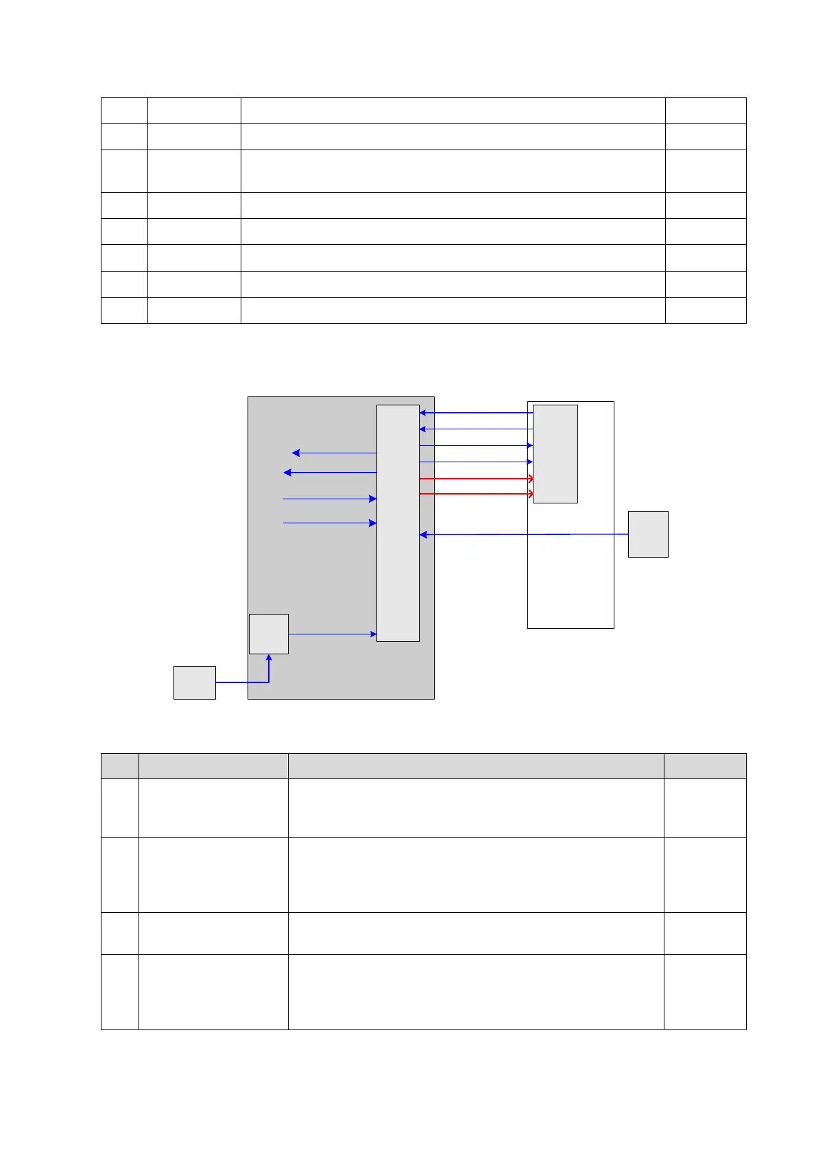
4.3.2 System Power-on Control
CPU
module
PWR_BTN_N
D12V
SUS_S3_N
SUS_S4_N
CPU_PWR_BTN_N
PWR_OK_N
5VSTB
Power
manag
ement
FPGA
AC-DC
Power
board
12V
AC in
place
signal
DC-DC power board
Main board
Control
panel
PWR_12V_EN
PWR_5VSTB_EN
PWR_5VSTB_OK_N
PWR_12V_OK_N
AC_IN_STATUS_N
Figure 6-12 Diagram of System Power-on Supported Circuit
Related controlling signal comment:
The pulse generated by the power button on the control
panel is sent to CPU module through power
management FPGA, to power on the system.
CPU module output effectively represents that CPU
system has been in the standby status, when 5VSTB
which is controlled by power management FPGA is in the
charging status.
CPU module output effectively represents that CPU
system has been in the dormancy status.
The output of power supply module is transmitted to the
CPU module by power management FPGA, which
represents the +12V output of power supply module has
been powered on.
 Loading...