32.3 Memory map/register description
This section provides a detailed description of all registers accessible in the PIT module.
NOTE
• Reserved registers will read as 0, writes will have no effect.
• See the chip configuration details for the number of PIT channels used in this MCU.
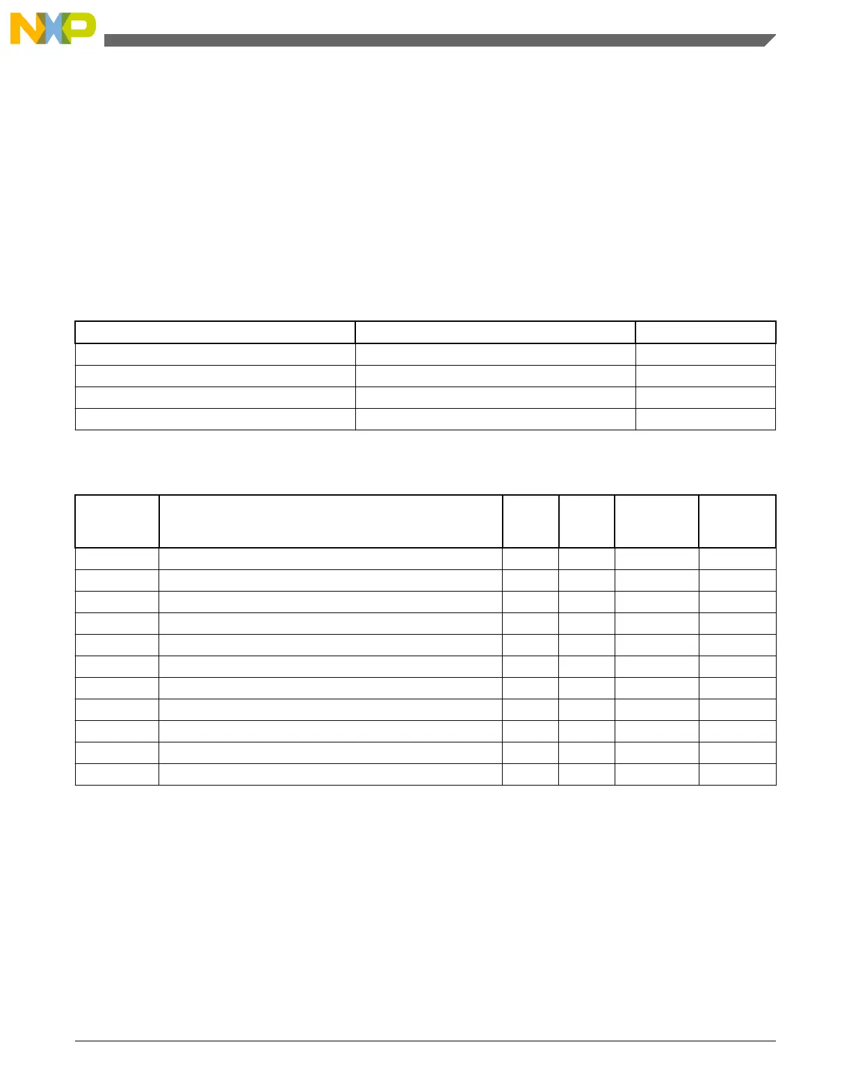
Table 32-2. Timer Channel n / RTI Channel
Address Offset Use Access
Channel + 0x00 Timer Load Value Register R/W
Channel + 0x04 Current Timer Value Register R
Channel + 0x08 Timer Control Register R/W
Channel + 0x0C Timer Flag Register R/W
PIT memory map
Absolute
address
(hex)
Register name
Width
(in bits)
Access Reset value
Section/
page
4003_7000 PIT Module Control Register (PIT_MCR) 32 R/W 0000_0002h 32.3.1/575
4003_70E0 PIT Upper Lifetime Timer Register (PIT_LTMR64H) 32 R 0000_0000h 32.3.2/577
4003_70E4 PIT Lower Lifetime Timer Register (PIT_LTMR64L) 32 R 0000_0000h 32.3.3/577
4003_7100 Timer Load Value Register (PIT_LDVAL0) 32 R/W 0000_0000h 32.3.4/578
4003_7104 Current Timer Value Register (PIT_CVAL0) 32 R 0000_0000h 32.3.5/578
4003_7108 Timer Control Register (PIT_TCTRL0) 32 R/W 0000_0000h 32.3.6/579
4003_710C Timer Flag Register (PIT_TFLG0) 32 R/W 0000_0000h 32.3.7/580
4003_7110 Timer Load Value Register (PIT_LDVAL1) 32 R/W 0000_0000h 32.3.4/578
4003_7114 Current Timer Value Register (PIT_CVAL1) 32 R 0000_0000h 32.3.5/578
4003_7118 Timer Control Register (PIT_TCTRL1) 32 R/W 0000_0000h 32.3.6/579
4003_711C Timer Flag Register (PIT_TFLG1) 32 R/W 0000_0000h 32.3.7/580
32.3.1 PIT Module Control Register (PIT_MCR)
This register enables or disables the PIT timer clocks and controls the timers when the
PIT enters the Debug mode.
Chapter 32 Periodic Interrupt Timer (PIT)
KL25 Sub-Family Reference Manual, Rev. 3, September 2012
Freescale Semiconductor, Inc. 575
 Loading...


