Pin Configuration 112 May 03, 2004
Philips Semiconductors Preliminary User Manual
LPC2119/2129/2194/2292/2294ARM-based Microcontroller
35
O
I
P0.10 RTS1 Request to Send output for UART1.
CAP1.0 Capture input for TIMER1, channel 0.
37
I
I
P0.11 CTS1 Clear to Send input for UART1.
CAP1.1 Capture input for TIMER1, channel 1.
38
I
O
I
P0.12 DSR1 Data Set Ready input for UART1.
MAT1.0 Match output for TIMER1, channel 0.
RD4 CAN4 receiver input (available in LPC2194 only).
39
O
O
O
P0.13 DTR1 Data Terminal Ready output for UART1.
MAT1.1 Match output for TIMER1, channel 1.
TD4 CAN4 transmitter output (available in LPC2194 only).
41
I
I
P0.14 DCD1 Data Carrier Detect input for UART1.
EINT1 External interrupt 1 input. LOW on this pine while RESET
is LOW
forces on-chip boot-loader to take over control of the part after reset.
Important: LOW on pin P0.14 while RESET
is LOW forces on-chip boot-loader to
take over control of the part after reset.
45
I
I
P0.15 RI1 Ring Indicator input for UART1.
EINT2 External interrupt 2 input.
46
I
O
I
P0.16 EINT0 External interrupt 0 input.
MAT0.2 Match output for TIMER0, channel 2.
CAP0.2 Capture input for TIMER0, channel 2.
47
I
I/O
O
P0.17 CAP1.2 Capture input for TIMER1, channel 2.
SCK1 Serial Clock for SPI1. SPI clock output from master or input to slave.
MAT1.2 Match output for TIMER1, channel 2.
53
I
I/O
O
P0.18 CAP1.3 Capture input for TIMER1, channel 3.
MISO1 Master In Slave Out for SPI1. Data input to SPI master or data output
from SPI slave.
MAT1.3 Match output for TIMER1, channel 3.
54
O
I/O
O
P0.19 MAT1.2 Match output for TIMER1, channel 2.
MOSI1 Master Out Slave In for SPI1. Data output from SPI master or data
input to SPI slave.
CAP1.2 Capture input for TIMER1, channel 2.
55
O
I
I
P0.20 MAT1.3 Match output for TIMER1, channel 3.
SSEL1 Slave Select for SPI1. Selects the SPI interface as a slave.
EINT3 External interrupt 3 input.
1
O
I
I
P0.21 PWM5 Pulse Width Modulator output 5.
RD3 CAN3 receiver input (available in LPC2194 only).
CAP1.3 Capture input for TIMER1, channel 3.
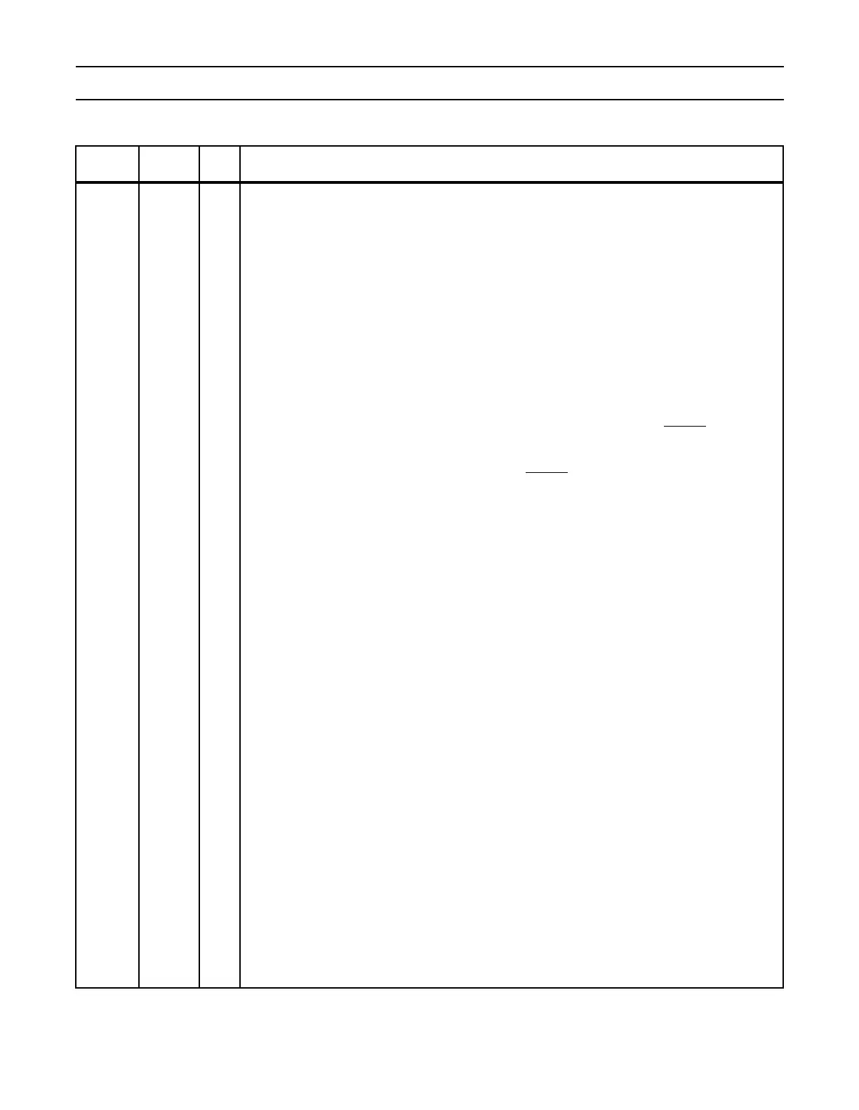
Table 55: Pin description for LPC2119/2129/2194
Pin
Name
LQFP64
Pin #
Type Description