RL78/F13, F14 CHAPTER 17 LIN/UART MODULE (RLIN3)
R01UH0368EJ0210 Rev.2.10 1110
Dec 10, 2015
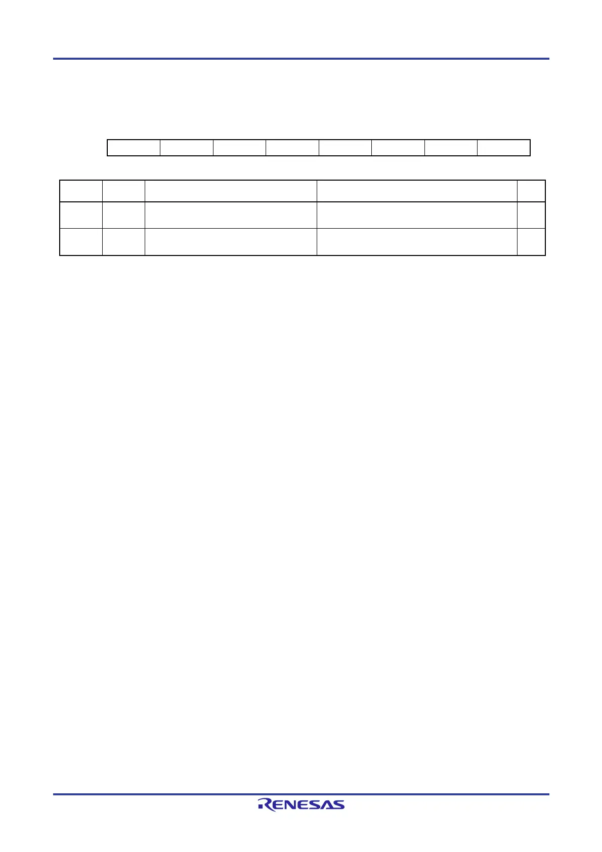
(2) LIN Channel Select Register (LCHSEL)
Address: F007BH
7 6 5 4 3 2 1 0
— — — — — — — LSEL0
Value after reset:
0 0 0 0 0 0 0 0
Bit Symbol Bit Name Function R/W
0 LSEL0 LIN Channel Select 0: Selects LIN0. (LIN0 registers can be accessed.)
1: Selects LIN1. (LIN1 registers can be accessed.)
R/W
7 to 1 — Reserved These bits are always read as 0. The write value
should always be 0.
R/W
LSEL0 bit (LIN channel select bit)
Since the LIN/UART module registers are not directly mapped on the CPU memory map, they should be accessed via the
register windows. The register windows are mapped on addresses F06C1H to F06E9H.
Setting a value to the LSEL0 bit maps all the registers of the corresponding channel on the register window.
Setting the LSEL0 bit to 0 maps the LIN0 registers.
Setting the LSEL0 bit to 1 maps the LIN1 registers.
With the product incorporating one channel, set the LSEL0 bit to 0.
With the product incorporating two channels, set the LSEL0 bit to the applicable value before accessing a register of the
channel to use.
 Loading...


