RL78/F13, F14 CHAPTER 6 TIMER ARRAY UNIT
R01UH0368EJ0210 Rev.2.10 443
Dec 10, 2015
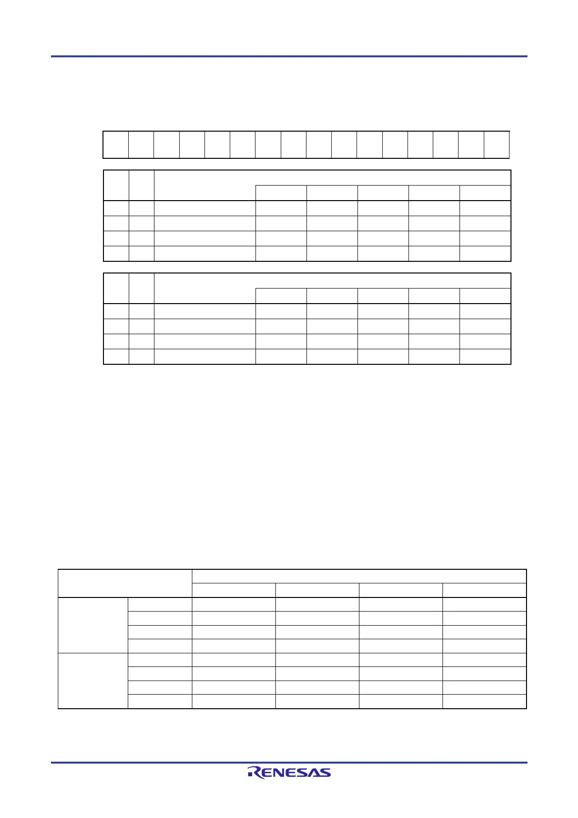
Figure 6-12. Format of Timer Clock Select Register 1 (TPS1) (4-ch version)
Address: F01F6H, F01F7H After reset: 0000H R/W
Symbol 15 14 13 12 11 10 9 8 7 6 5 4 3 2 1 0
TPSm 0 0
PRS
131
PRS
130
0 0
PRS
121
PRS
120
PRS
113
PRS
112
PRS
111
PRS
110
PRS
103
PRS
102
PRS
101
PRS
100
PRS
121
PRS
120
Selection of operation clock (CK12)
Note
fCLK = 2 MHz fCLK = 5 MHz fCLK = 10 MHz fCLK = 20 MHz fCLK = 32 MHz
0 0 fCLK/2 1 MHz 2.5 MHz 5 MHz 10 MHz 16 MHz
0 1 fCLK/2
2
500 kHz 1.25 MHz 2.5 MHz 5 MHz 8 MHz
1 0 fCLK/2
4
125 kHz 312.5 kHz 625 kHz 1.25 MHz 2 MHz
1 1 fCLK/2
6
31.25 kHZ 78.1 kHz 156.2 kHz 312.5 kHz 500 kHZ
PRS
131
PRS
130
Selection of operation clock (CK13)
Note
fCLK = 2 MHz fCLK = 5 MHz fCLK = 10 MHz fCLK = 20 MHz fCLK = 32 MHz
0 0 fCLK/2
8
7.81 kHz 19.5 kHz 39.1 kHz 78.1 kHz 125 kHz
0 1 fCLK/2
10
1.95 kHz 4.88 kHz 9.76 kHz 19.5 kHz 31.25 kHz
1 0 fCLK/2
12
488 Hz 1.22 kHz 2.44 kHz 4.88 kHz 7.81 kHz
1 1 fCLK/2
14
122 HZ 305 Hz 610 Hz 1.22 kHz 1.95 kHZ
Note The above format is applied to the TPS1 of the Group B, C, and D products.
When changing the clock selected for f
CLK (by changing the system clock control register (CKC) value), stop timer
array unit (TTm = 00FFH).
The timer array unit must also be stopped if the operating clock (f
MCK) specified by using the CKSmn0, and
CKSmn1 bits or the valid edge of the signal input from the TImn pin is selected as the count clock (f
TCLK).
Cautions 1. This format cannot be applied to the Group A and E products and unit 0 of the Group B, C, and D
products (see the specifications of 8-channel version in Figure 6-11).
2. When selecting f
CLK (not divided) as the operation clock (CKmk) and setting TDRnm = 0000H (n =
0, 1; m = 0 to 7), set the interrupt mask flag to “interrupt processing disabled” (TMMKnm = 1).
By using channels 1 and 3 in the 8-bit timer mode and specifying CKm2 or CKm3 as the operation clock, the interval
times shown in Table 6-4 can be achieved by using the interval timer function.
Table 6-4. Interval Times Available for Operation Clock CKSm2 or CKSm3
Clock
Interval time (f
CLK = 32 MHz)
Note
10 s 100
s 1 ms 10 ms
CKm2 fCLK/2
fCLK/2
2
fCLK/2
4
fCLK/2
6
CKm3 fCLK/2
8
fCLK/2
10
fCLK/2
12
fCLK/2
14
Note The margin is within 5 %.
Remarks 1. fCLK: CPU/peripheral hardware clock frequency
2. For details of a signal of f
CLK/2
i
selected with the TPSm register, see 6.5.1 Count clock (fTCLK).
 Loading...


