RL78/F13, F14 CHAPTER 6 TIMER ARRAY UNIT
R01UH0368EJ0210 Rev.2.10 445
Dec 10, 2015
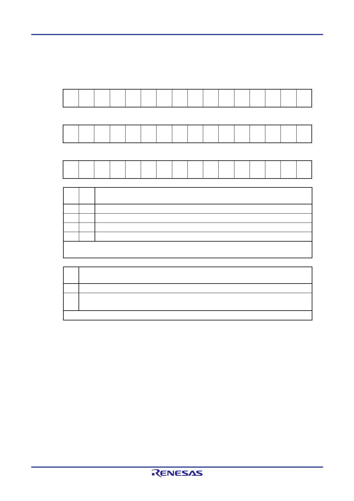
Figure 6-13. Format of Timer Mode Register mn (TMRmn) (1/4)
Address: F0190H, F0191H (TMR00) to F019EH, F019FH (TMR07), After reset: 0000H R/W
F01D0H, F01D1H (TMR10) to F01DEH, F01DFH (TMR17)
Symbol 15 14 13 12 11 10 9 8 7 6 5 4 3 2 1 0
TMRmn
(n = 2, 4, 6)
CKS
mn1
CKS
mn0
0
CCS
mn
MAST
ERmn
STS
mn2
STS
mn1
STS
mn0
CIS
mn1
CIS
mn0
0 0
MD
mn3
MD
mn2
MD
mn1
MD
mn0
Symbol 15 14 13 12 11 10 9 8 7 6 5 4 3 2 1 0
TMRmn
(n = 1, 3)
CKS
mn1
CKS
mn0
0
CCS
mn
SPLIT
mn
STS
mn2
STS
mn1
STS
mn0
CIS
mn1
CIS
mn0
0 0
MD
mn3
MD
mn2
MD
mn1
MD
mn0
Symbol 15 14 13 12 11 10 9 8 7 6 5 4 3 2 1 0
TMRmn
(n = 0, 5, 7)
CKS
mn1
CKS
mn0
0
CCS
mn
0
Note
STS
mn2
STS
mn1
STS
mn0
CIS
mn1
CIS
mn0
0 0
MD
mn3
MD
mn2
MD
mn1
MD
mn0
CKS
mn1
CKS
mn0
Selection of operation clock (f
MCK) of channel n
0 0 Operation clock CKm0 set by timer clock select register m (TPSm)
0 1 Operation clock CKm2 set by timer clock select register m (TPSm)
1 0 Operation clock CKm1 set by timer clock select register m (TPSm)
1 1 Operation clock CKm3 set by timer clock select register m (TPSm)
Operation clock (fMCK ) is used by the edge detector. A count clock (fTCLK) and a sampling clock are generated
depending on the setting of the CCSmn bit.
CCS
mn
Selection of count clock (f
TCLK) of channel n
0 Operation clock (fMCK) specified by the CKSmn0 and CKSmn1 bits
1 Valid edge of input signal input from the TImn pin
Valid edge of input signal selected by TIS0 in channel 5
Count clock (fTCLK) is used for the timer/counter, output controller, and interrupt controller.
Note Bit 11 is a read-only bit and fixed to 0. Writing to this bit is ignored.
Cautions 1. Be sure to clear bits 13, 5, and 4 to “0”.
2. The timer array unit must be stopped (TTm = 00FFH) if the clock selected for fCLK is changed
(by changing the value of the system clock control register (CKC)), even if the operating clock
specified by using the CKSmn0 and CKSmn1 bits (f
MCK) or the valid edge of the signal input
from the TImn pin is selected as the count clock (fTCLK).
3. Be sure to clear CKS1n0 (n = 0, 2) to “0” in the Group B, C, and D products.
Remarks 1. m: Unit number (m = 0, 1), n: Channel number (n = 0 to 7)
2. TMR1n is not provided in the Group A products.
TMR17 to TMR14 are not provided in the Group B, C, and D products.
 Loading...


