RL78/F13, F14 CHAPTER 8 TIMER RD
R01UH0368EJ0210 Rev.2.10 646
Dec 10, 2015
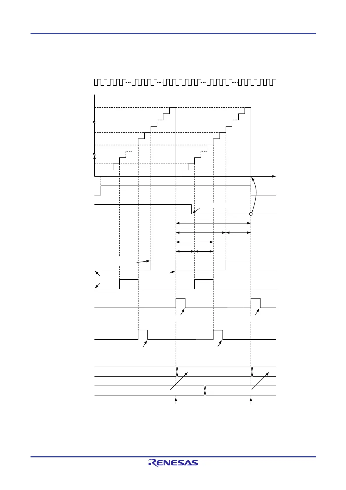
(1) Operation Example
Figure 8-61. Operation Example in PWM3 Mode
m + 1
n + 1
0000H
FFFFH
m - n
p + 1
q + 1
m
n
p
q
p - q
m
m
m
Count source
Value in TRD0 register
TSTART0 bit in
TRDSTR register
CSEL0 bit in
TRDSTR register
TRDIOA0 output
TRDIOB0 output
Initial output is
low
IMFB bit in
TRDSR0 register
0TRDGRA0 register
TRDGRC0 register
Remark
j = A or B
m: Value set in TRDGRA0 register
n: Value set in TRDGRA1 register
p: Value set in TRDGRB0 register
q: Value set in TRDGRB1 register
Transfer from buffer register
to general register
Transfer from buffer register
to general register
Following data
Transfer Transfer
Set to 0 by a programSet to 0 by a program
Set to 0 by a program
Initial output is
low
High output by compare
match with TRDGRA1
register
Low output by compare
match with TRDGRA0
register
Count stops
Set to 0 by a program
Time
Set to 0 by a program
The above diagram applies under the following conditions :
The above diagram applies under the following conditions :
• Both the TOA0 and TOB0 bits in the TRDOCR register are set to 0 (initial output is low, high output by compare
match with TRDGRj1 register, low output by compare match with TRDGRj0 register).
• The TRDBFC0 bit in the TRDMR register is set to 1 (TRDGRC0 register is buffer register for TRDGRA0 register).
 Loading...


