RL78/F13, F14 CHAPTER 12 A/D CONVERTER
R01UH0368EJ0210 Rev.2.10 708
Dec 10, 2015
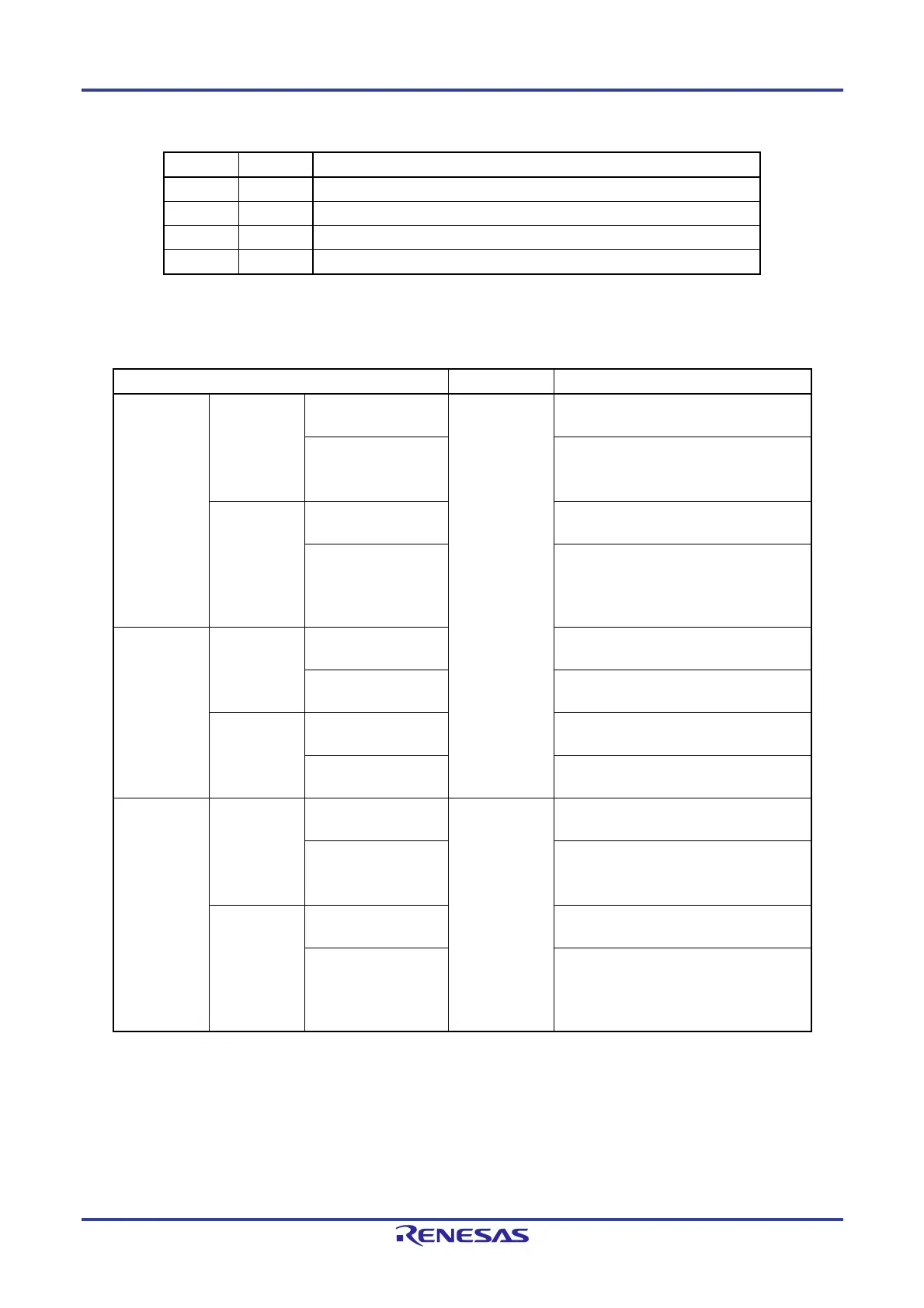
Table 12-1. Settings of ADCS and ADCE Bits
ADCS ADCE A/D Conversion Operation
0 0 Stop status (DC power consumption path does not exist)
0 1
Conversion standby mode (only A/D voltage comparator consumes power
Note
)
1 0 Setting prohibited
1 1 Conversion mode (A/D voltage comparator: enables operation)
Note In hardware trigger wait mode, there is no DC power consumption path even during conversion standby
mode.
Table 12-2. Setting and Clearing Conditions for ADCS Bit
A/D Conversion Mode Set Conditions Clear Conditions
Software
trigger
Select mode
Sequential conversion
mode
When 1 is
written to ADCS
When 0 is written to ADCS
One-shot conversion
mode
When 0 is written to ADCS
The bit is automatically cleared to 0 when
A/D conversion ends.
Scan mode
Sequential conversion
mode
When 0 is written to ADCS
One-shot conversion
mode
When 0 is written to ADCS
The bit is automatically cleared to 0 when
conversion ends on the specified four
channels.
Hardware
trigger no-wait
mode
Select mode
Sequential conversion
mode
When 0 is written to ADCS
One-shot conversion
mode
When 0 is written to ADCS
Scan mode
Sequential conversion
mode
When 0 is written to ADCS
One-shot conversion
mode
When 0 is written to ADCS
Hardware
trigger wait
mode
Select mode
Sequential conversion
mode
When a
hardware trigger
is input
When 0 is written to ADCS
One-shot conversion
mode
When 0 is written to ADCS
The bit is automatically cleared to 0 when
A/D conversion ends.
Scan mode
Sequential conversion
mode
When 0 is written to ADCS
One-shot conversion
mode
When 0 is written to ADCS
The bit is automatically cleared to 0 when
conversion ends on the specified four
channels.
 Loading...


