RL78/F13, F14 CHAPTER 12 A/D CONVERTER
R01UH0368EJ0210 Rev.2.10 709
Dec 10, 2015
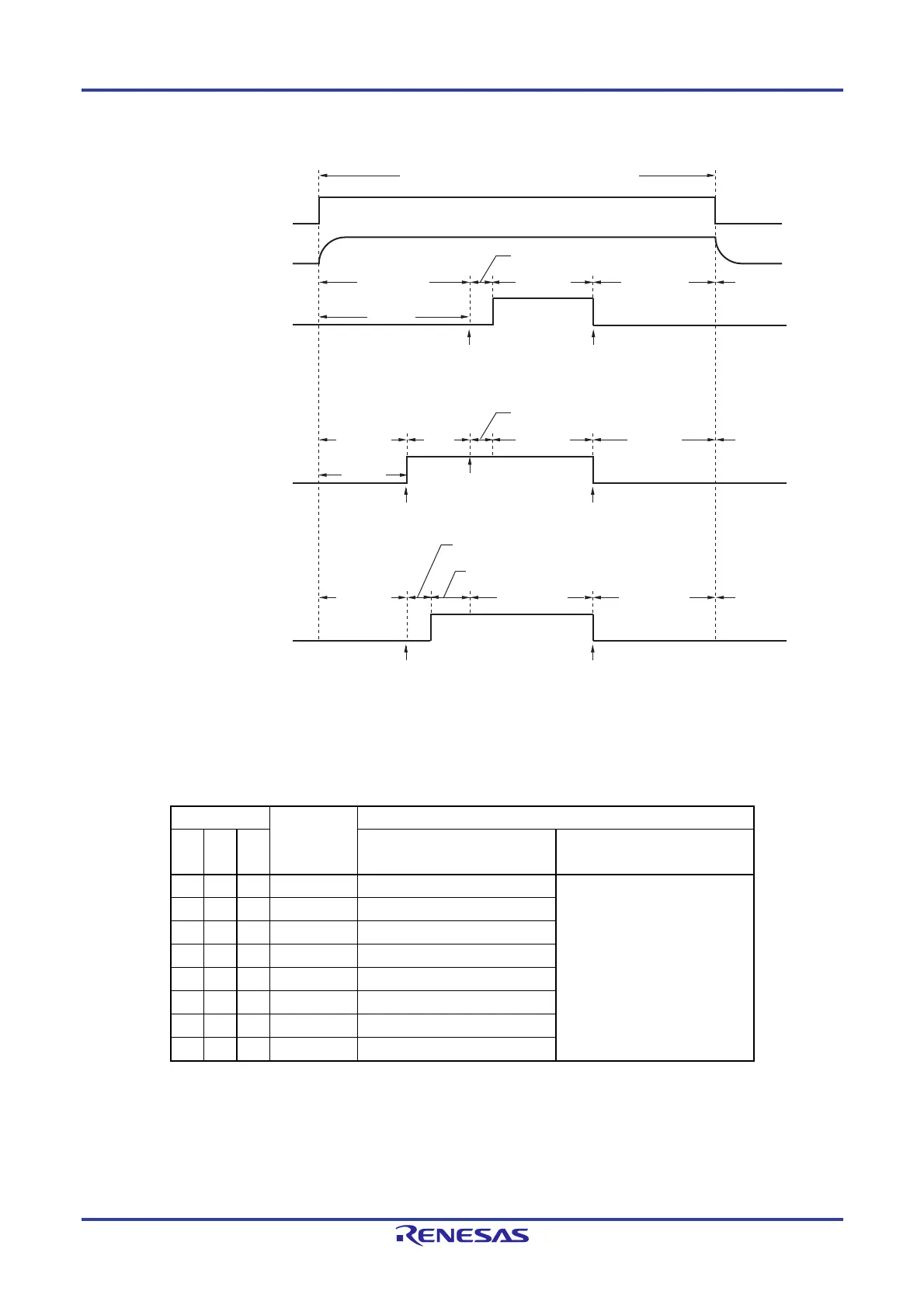
Figure 12-4. Timing Chart When A/D Voltage Comparator Is Used
Notes 1. While in the software trigger mode or hardware trigger no-wait mode, the time from the rising of the ADCE bit
to the falling of the ADCS bit must be 1 s or longer to stabilize the internal circuit.
2. The following time is the maximum amount of time necessary to start conversion.
ADM0 Conversion
Clock
(f
AD)
Conversion Start Time (Number of fCLK Clocks)
FR2 FR1 FR0 Software trigger mode/
Hardware trigger no wait mode
Hardware trigger wait mode
0 0 0 fCLK/64 63 1
0 0 1 fCLK/32 31
0 1 0 fCLK/16 15
0 1 1 fCLK/8 7
1 0 0 fCLK/6 5
1 0 1 fCLK/5 4
1 1 0 fCLK/4 3
1 1 1 fCLK/2 1
However, for the second and subsequent conversion in sequential conversion mode and for conversion of the
channel specified by scan 1, 2, and 3 in scan mode, the conversion start time and stabilization wait time for
A/D power supply do not occur after a hardware trigger is detected.
Remark f
CLK: CPU/peripheral hardware clock frequency
ADCE
ADCS
Conversion
standby
ADCS
ADCS
A/D power stabilization
wait time
A/D voltage comparator: enables operation
A/D voltage comparator
Software
trigger mode
Conversion
standby
Conversion start time
Note 2
Conversion
operation
Conversion
stopped
Hardware trigger
no-wait mode
Hardware trigger
wait mode
Note 1
1 is written
to ADCS.
0 is written
to ADCS.
This bit is automatically cleared to 0
after A/D conversion ends.
Conversion start time
Note 2
Conversion
standby
Trigger
standby
Conversion
operation
Conversion
standby
Conversion
stopped
Note 1
Hardware
trigger detection
1 is written
to ADCS.
0 is written
to ADCS.
Conversion start time
Note 2
Conversion
standby
Conversion
operation
0 is written
to ADCS.
This bit is automatically cleared to 0
after A/D conversion ends.
Hardware trigger
detection
Conversion
standby
Conversion
stopped
 Loading...


