Table of figures
Table of figures
Figure 1 BENNINGST755+/ BENNINGST760+ device structure .............................................................. 21
Figure 2 Type plate (exemplary) ..................................................................................................................... 22
Figure 3 Screen layout.................................................................................................................................... 23
Figure 4 General operation ............................................................................................................................. 29
Figure 5 Test view........................................................................................................................................... 31
Figure 6 BENNINGMA4 ................................................................................................................................ 49
Figure 7 BENNINGMA3 ................................................................................................................................ 50
Figure 8 BENNINGMA2-16........................................................................................................................... 50
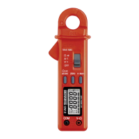
Figure 9 BENNINGCM9-1/ BENNINGCM9-2 ............................................................................................ 51
Figure 10Balance/ calibration ......................................................................................................................... 69
Figure 11Device view– jacks .......................................................................................................................... 75
Figure 12Testing the protective conductor resistance (connection diagram exemplary for VDE0701 and
VDE0702, circuit diagram)............................................................................................................... 79
Figure 13Testing the insulating resistance, ClassI (connection diagram exemplary for VDE0701 and
VDE0702, circuit diagram)............................................................................................................... 80
Figure 14Testing the insulating resistance, ClassII (connection diagram exemplary for VDE0701 and
VDE0702, circuit diagram)............................................................................................................... 81
Figure 15Testing the insulating resistance, ClassIII (connection diagram exemplary for VDE0701 and
VDE0702, circuit diagram)............................................................................................................... 82
Figure 16Testing the protective conductor current (connection diagram, circuit diagram) .............................. 83
Figure 17Testing the contact current, ClassI (connection diagram exemplary for VDE0701 and VDE0702,
circuit diagram) ................................................................................................................................ 84
Figure 18Testing the contact current, ClassII (connection diagram exemplary for VDE0701 and
VDE0702, circuit diagram)............................................................................................................... 85
Figure 19Testing the device leakage current (connection diagram for VDE0751-1, circuit diagram)............. 86
Figure 20Testing the patient leakage current, ClassI (connection diagram for VDE0751-1, circuit diagram,
applied parts of typeF) ..................................................................................................................... 88
Figure 21Testing the patient leakage current, ClassII (connection diagram for VDE0751-1, circuit dia-
gram, applied parts of typeF)........................................................................................................... 88
Figure 22Functional test (connection diagram, circuit diagram) ...................................................................... 90
Figure 23Cable continuity test (example: multiple socket, connection diagram, circuit diagram).................... 91
Figure 24Testing the safety extra-low voltage, ClassI (connection diagram, circuit diagram)........................ 92
Figure 25Testing the voltage of the welding circuit (connection diagram, circuit diagram).............................. 93
Figure 26Testing the contact current of the welding circuit (connection diagram, circuit diagram) ................. 94
Figure 27Testing of PRCDs (connection diagram) .......................................................................................... 95
5284 / 08/2023 en BENNING ST 755+ / ST 760+ 7