Titanium Interfaces User Guide
Table 80: PLL Manual Mode Options
Option Choices Description
Pre-Divider (N) 1, 2, 4 The pre-divider value.
Multiplier (M) 1, 2, 4 The multiplier value.
Post-Divider (O) 1, 2, 4, 8, 16, 32, 64, 128 Post-divider value.
CLK Divider n 1 - 128 Clock divider for each output.
Phase Shift Value n 0 - 7 Post-divider VCO cycle delay
to phase shift, in degrees:
0: No phase shift
1: 0.5
2: 1
3: 1.5
4: 2
5: 2.5
6: 3
7: 3.5
The post-divider VCO cycle delay relates to the phase shift as shown in the following
equation:
Phase shift (in degrees) = ( (Post-divider VCO cycle delay x O x F
CLKOUT
) / F
VCO
) x 360
where:
• O is the post-VCO division ration
• F
CLKOUT
is the output frequency
• F
VCO
is the VCO frequency
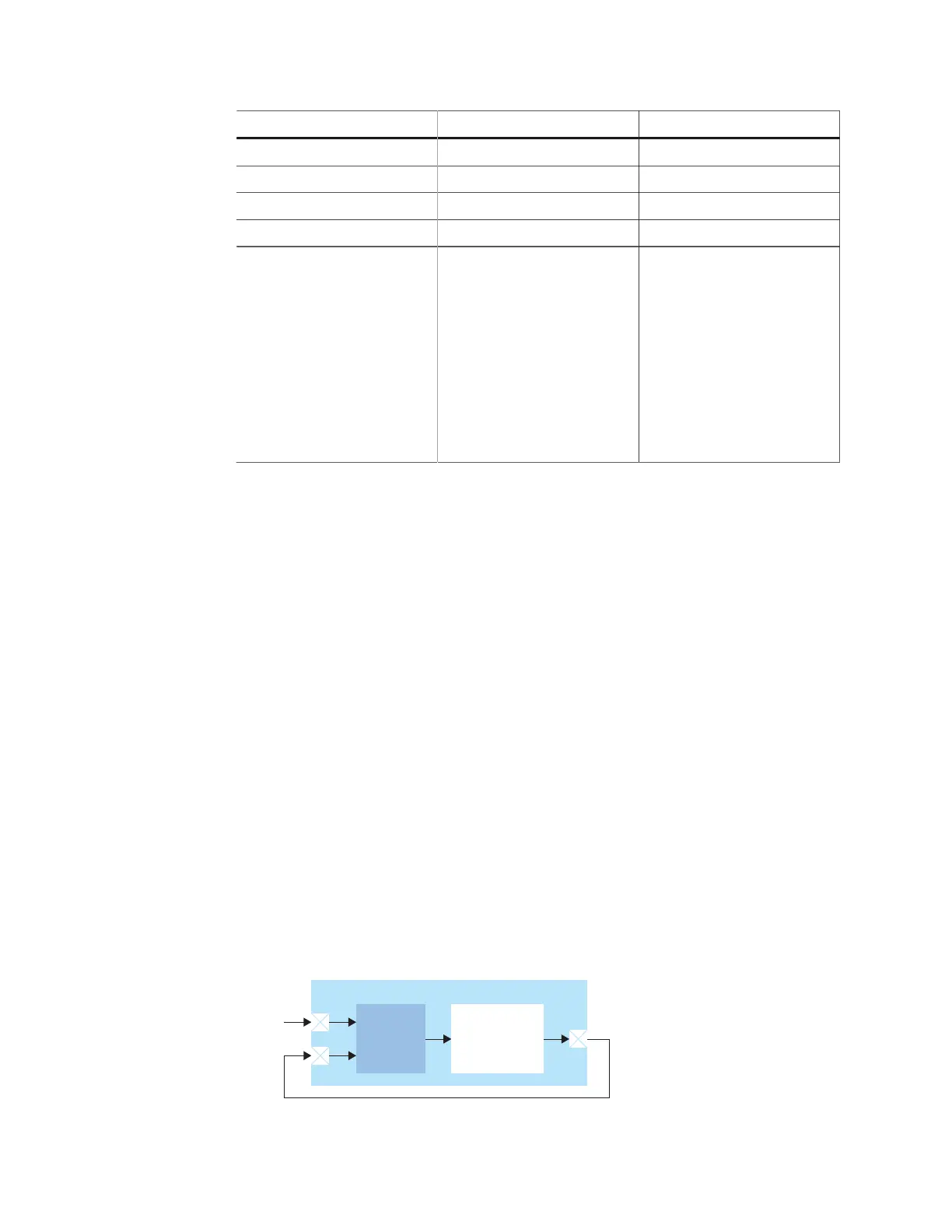
Implementing a Zero-Delay Buffer
Titanium PLLs can implement a zero-delay buffer circuit. In this mode, the PLL removes all
of the clock-insertion delay from the input I/O buffer and core clock tree. You may want to
use this buffer when you have a single clock signal that fans out to more than one destination
with low skew.
To implement a zero-delay buffer:
• In the PLL Clock Calculator, use Feedback Mode > External.
• Add a GPIO for the clock output.
• Add a second GPIO for the external feedback.
• Add a third GPIO for the PLL reference clock.
• On your board, connect the clock output pin to the external feedback pin.
Figure 51: Zero-Delay Buffer Block Diagram
Choose the location of the clkout and extfb pins to minimize
any board delay.
www.efinixinc.com 125