Titanium Interfaces User Guide
Chapter 7
HyperRAM Interface
Contents:
• About the HyperRAM
• Using the HyperRAM Interface
The Ti35 and Ti60 FPGAs in the F100 package include an integrated HyperRAM memory.
You use the Interface Designer to connect this block to your user design. Only the Ti35 or
Ti60 can communicate with the on-board HyperRAM.
About the HyperRAM
The Titanium FPGA in F100S3F2 package includes a HyperRAM. The HyperRAM has a
density of 256 Mbits and a clock rate of up to 250 MHz. The HyperRAM supports double-
data rates of up to 500 Mbps and supports a 16 bit data bus.
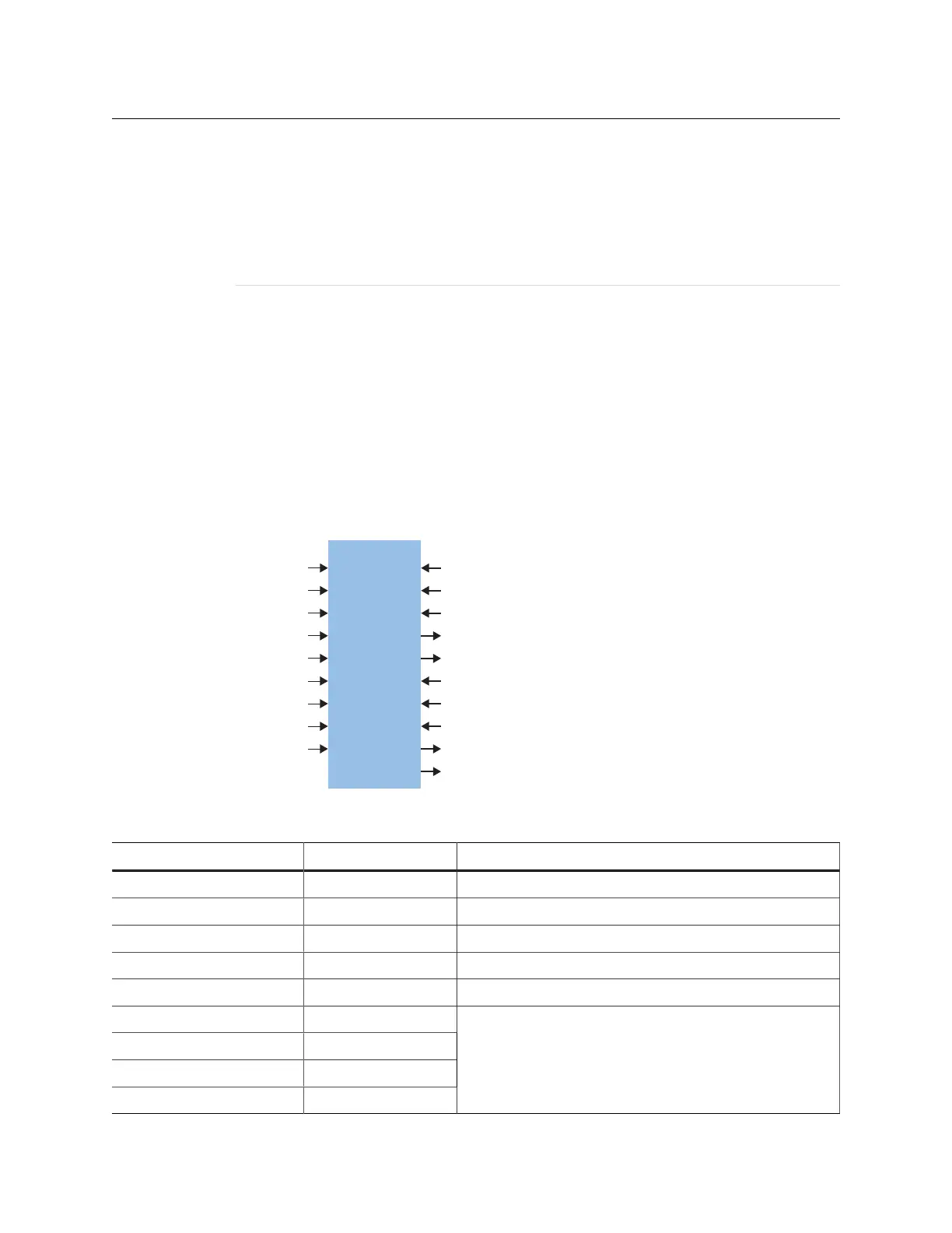
Figure 29: HyperRAM Block Diagram
CLK
CLK90
CLKCAL
RST_N
CS_N
CK_P_HI
CK_P_LO
CK_N_HI
CK_N_LO
RWDS_OUT_HI [1:0]
RWDS_OUT_LO [1:0]
RWDS_OE [1:0]
RWDS_IN_HI [1:0]
RWDS_IN_LO [1:0]
DQ_OUT_HI [15:0]
DQ_OUT_LO [15:0]
DQ_OE [15:0]
DQ_IN_HI [15:0]
DQ_IN_LO [15:0]
Table 45: HyperRAM Signals (Interface to FPGA Fabric)
Signal Direction Description
CLK Input HyperRAM controller clock.
CLK90 Input 90 degree phase-shifted version of CLK.
CLKCAL Input Calibration clock for input data.
RST_N Input Active-low HyperRAM reset.
CS_N Input Active-low HyperRAM chip select signal.
CK_P_HI Input
CK_P_LO Input
CK_N_HI Input
CK_N_LO Input
The clock provided to the HyperRAM. The clock is not
required to be free-running. Registered in normal mode of
DDIO.
www.efinixinc.com 86