Titanium Interfaces User Guide
Double-Data I/O
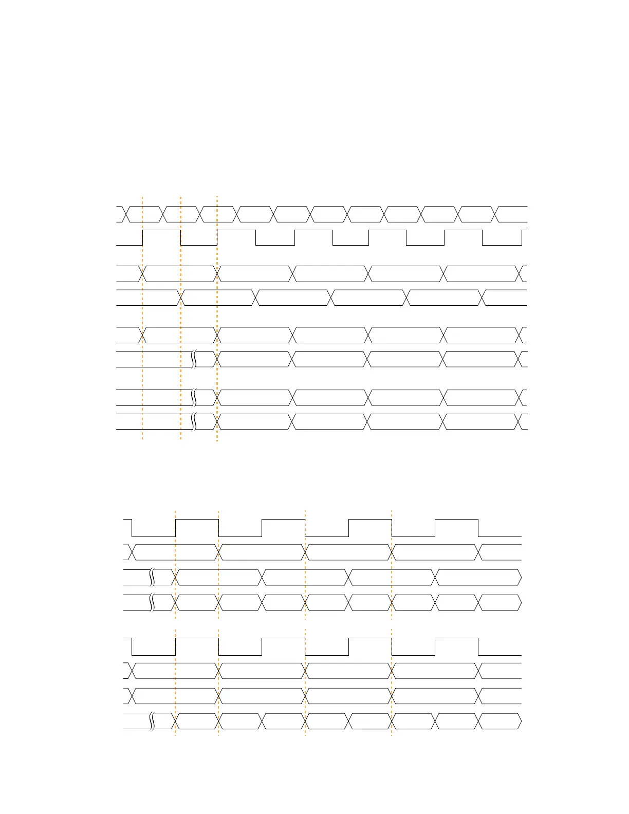
Titanium FPGAs support double data I/O (DDIO) on input and output registers. In this
mode, the DDIO register captures data on both positive and negative clock edges. The core
receives 2 bit wide data from the interface.
In normal mode, the interface receives or sends data directly to or from the core on the
positive and negative clock edges. In resync and pipeline mode, the interface resynchronizes
the data to pass both signals on the positive clock edge only.
Figure 12: DDIO Input Timing Waveform
In resync mode, the IN1 data captured on the falling clock edge is delayed one half clock cycle.
In the Interface Designer, IN0 is the HI pin name and IN1 is the LO pin name.
Figure 13: DDIO Output Timing Waveform
DATA1 DATA2 DATA3 DATA4 DATA5 DATA6 DATA7
DATA4 DATA6 DATA8
DATA1 DATA2 DATA3 DATA4 DATA5 DATA6 DATA7
DATA4 DATA6 DATA8
In the Interface Designer, OUT0 is the HI pin name and OUT1 is the LO pin name.
www.efinixinc.com 42