Titanium Interfaces User Guide
I/O Banks Interface
The I/O Banks setting shows the device I/O banks and the I/O voltage each bank uses.
Some I/O banks support multiple I/O standards, and you can specify which standard the
bank uses. These settings determine the FPGA pinout requirements and timing values of
the interface blocks. Some I/O banks can support multiple I/O standards as long as the I/O
voltages of the different standards are compatible.
To set the I/O voltage for a bank:
1. Click Device Setting > I/O Banks.
2. In the Block Editor, select the I/O voltage for the bank.
You also select an I/O standard for GPIO blocks. The voltage you select for the I/O bank
must be compatible with the settings you choose for any GPIO in this bank.
3. Save.
Note: The I/O banks and their legal configuration are device and package specific. Refer to the data sheet
for your chosen FPGA for details on which I/O standards it supports.
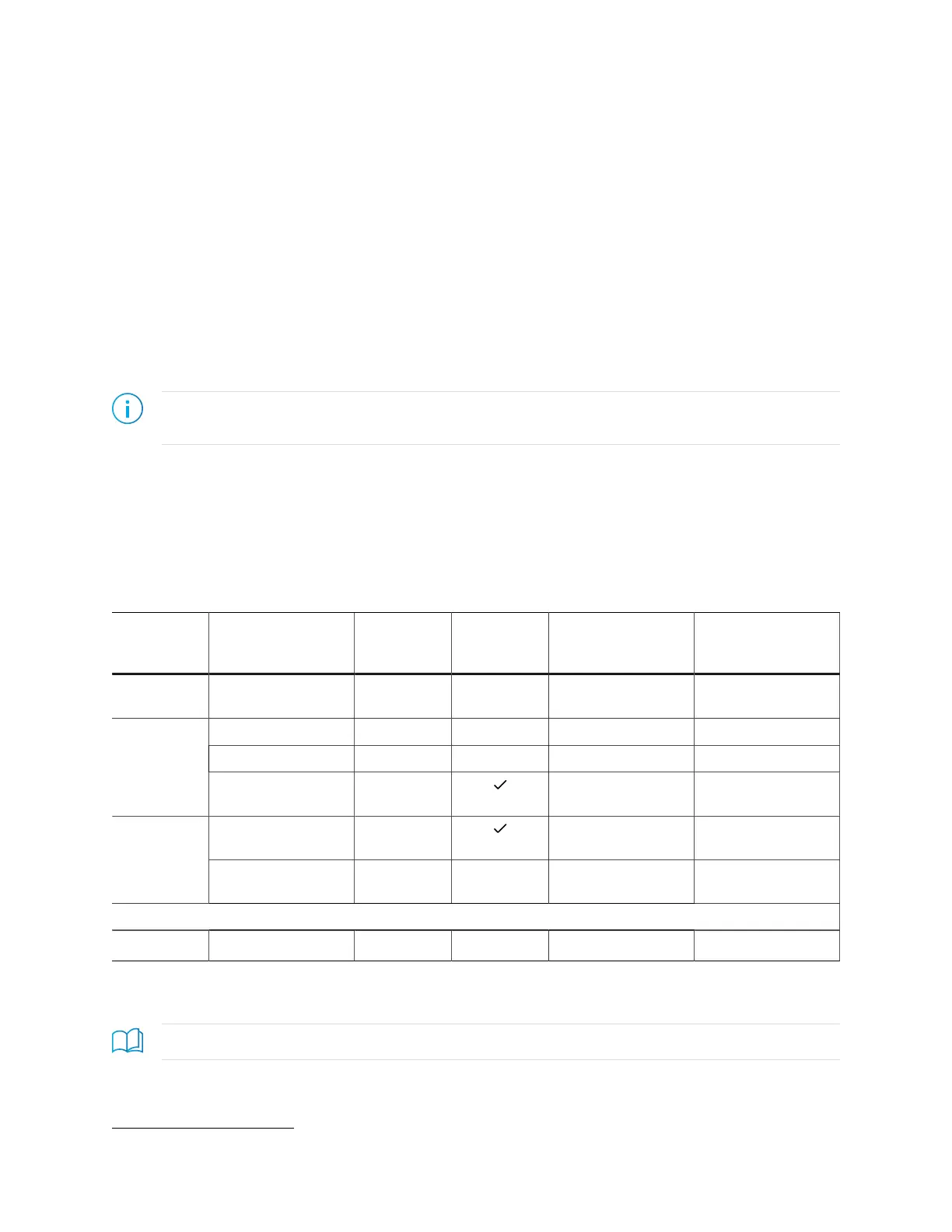
Titanium I/O Banks
Efinix FPGAs have input/output (I/O) banks for general-purpose usage. Each I/O bank has
independent power pins. The number and voltages supported vary by FPGA and package.
Table 5: Titanium I/O Banks by FPGA and Package
Package I/O Banks Voltage (V) Dynamic
Voltage
Support
DDIO Support Merged Banks
W64 1A, 1B, 2A, 3B 1.2, 1.5, 1.8 – All 1A_4B, 1B_2A,
2A_3A_3B_4A
1A, 2A, 2B, 4B 1.8 – All 1A_4B, 2A_2B
1B, 3A, 3B, 4A 1.2, 1.5, 1.8 – All 3B_4A
F100S3F2
BL 1.8, 2.5,
3.0, 3.3
All –
BL, TL, TR, BR, 1.8, 2.5,
3.0, 3.3
All –F225
1A, 1B, 2A, 2B,
3A, 3B, 4A, 4B
1.2, 1.5, 1.8 – All –
Ti90, Ti135, Ti180
M484
(3) (3) (3) (3) (3)
Some I/O banks are merged at the package level by sharing VCCIO pins. Merged banks have
underscores (_) between banks in the name (e.g., 1B_1C means 1B and 1C are connected).
Learn more: Refer to the FPGA pinout for information on the I/O bank assignments.
(3)
Pending definition.
www.efinixinc.com 21