Titanium Interfaces User Guide
Option Description
Output pin/
bus name
Any
Parallel clock
division
1: The output clock from the LVDS TX lane is parallel clock
frequency.
2: The output clock from the TX lane is half of the parallel clock
frequency.
Serial clock
pin name
Specify the fast clock output name that corresponds to the PLL you
chose.
Parallel clock
pin name
Use the slow clock output name that corresponds to the PLL you
chose.
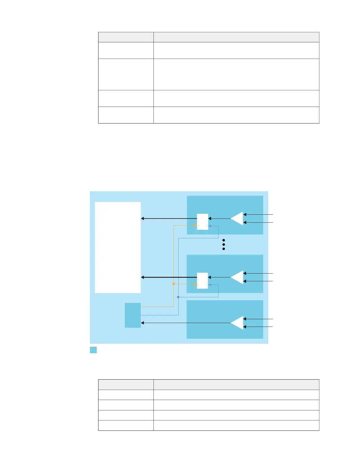
Create an LVDS RX Interface
The following figure shows a completed LVDS RX interface, where n is the deserialization
width and m is the number of RX lanes.
Figure 28: Complete LVDS RX Interface Block Diagram
SLOWCLK
FASTCLK
Receiver
LVDS RX Clock Input
Follow these steps to build an LVDS RX interface using the Efinity
®
Interface Designer.
1. Add an LVDS RX block to act as the PLL reference clock input:
Option Description
LVDS Type Receiver (RX)
LVDS Resource T13/T20 BGA169 and BGA256 only: GPIOB_CLK0.lvds
Connection Type pll_clkin
Input Pin/Bus Name Use the clock LVDS RX clock output name as the incoming clock.
www.efinixinc.com 77