Titanium Interfaces User Guide
Chapter 11
PLL
Contents:
• About the PLL Interface
• Using the PLL V3 Block
• Implementing a Zero-Delay Buffer
• Design Check: PLL Errors
About the PLL Interface
Titanium FPGAs have PLLs to synthesize clock frequencies. The PLLs are located in the
corners of the FPGA. You can use the PLL to compensate for clock skew/delay via external
or internal feedback to meet timing requirements in advanced application. The PLL reference
clock has up to four sources. You can dynamically select the PLL reference clock with the
CLKSEL port. (Hold the PLL in reset when dynamically selecting the reference clock source.)
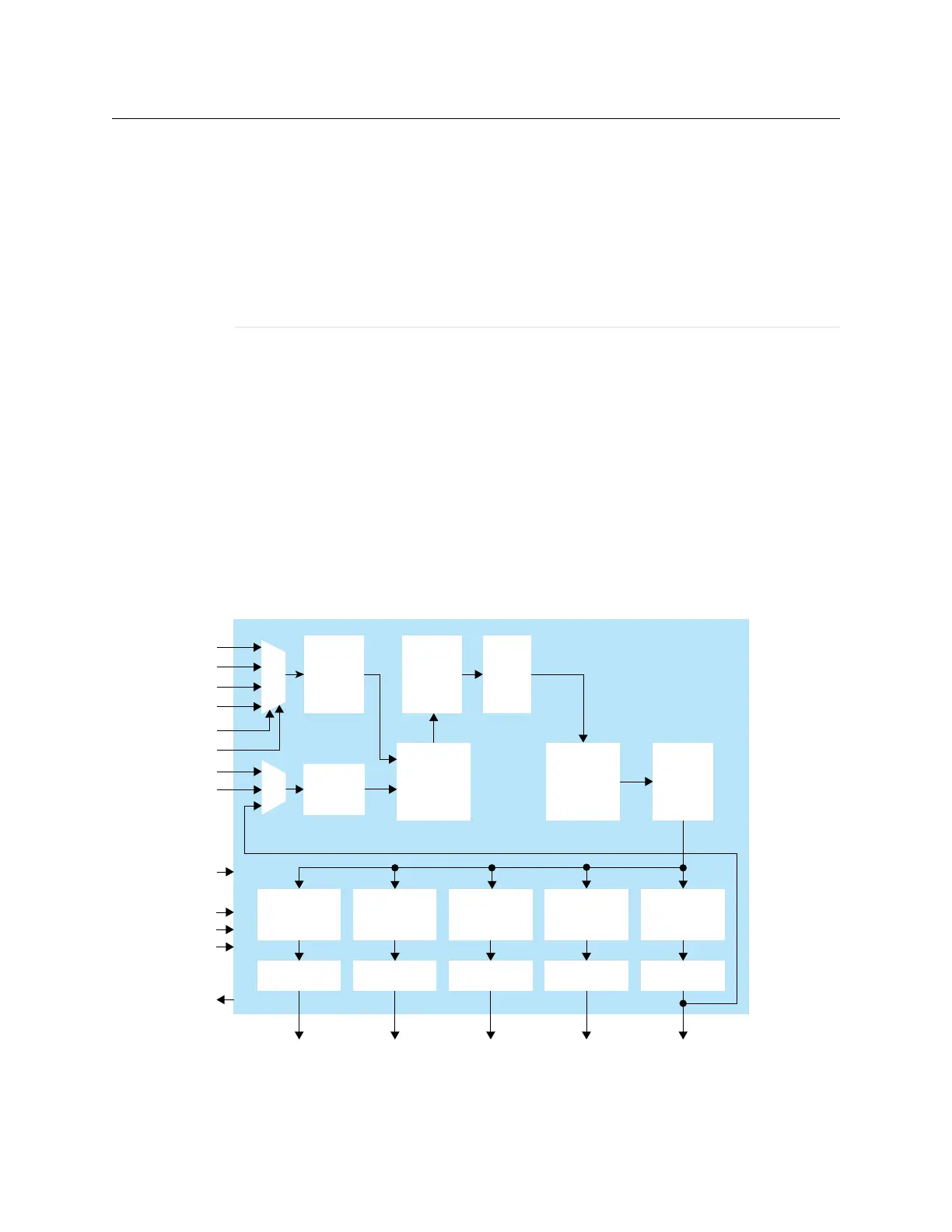
The PLL consists of a pre-divider counter (N counter), a feedback multiplier counter (M
counter), a post-divider counter (O counter), and output dividers (C).
Figure 48: PLL Block Diagram
Voltage
Control
Oscillator
O
Counter
CLKIN[3]
CLKIN[2]
CLKIN[1]
CLKIN[0]
Output
Divider (C)
Phase Shift
CLKOUT3
Output
Divider (C)
Phase Shift
CLKOUT2
Output
Divider (C)
Phase Shift
CLKOUT1
Output
Divider (C)
Phase Shift
CLKOUT0
SHIFT[2:0]
SHIFT_SEL[4:0]
SHIFT_ENA
The counter settings define the PLL output frequency:
www.efinixinc.com 121