Titanium Interfaces User Guide
Chapter 14
Interface Floorplans
Note: The numbers in the floorplan figures indicate the HVIO and HSIO number ranges. Some packages
may not have all HVIO or HSIO pins in the range bonded out.
Floorplan Diagram for FPGAs in W64 Packages
Figure 53: Ti60 FPGAs
Quantum
Compute Fabric
Dimensions not to scale
Dedicated blocks
PLL
HSIO
0
3B
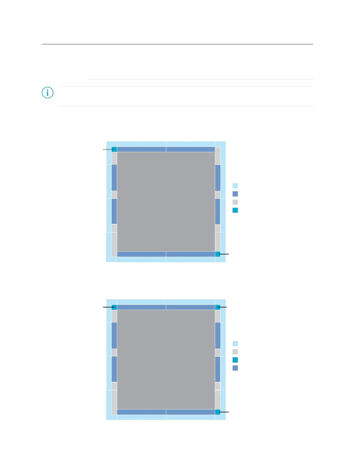
Floorplan Diagram for FPGAs in F100 Packages
Figure 54: Ti35 and Ti60 FPGAs
Quantum
Compute Fabric
Dimensions not to scale
I/O bank
Dedicated blocks
PLL
HSIO
0
3B
www.efinixinc.com 135