Titanium Interfaces User Guide
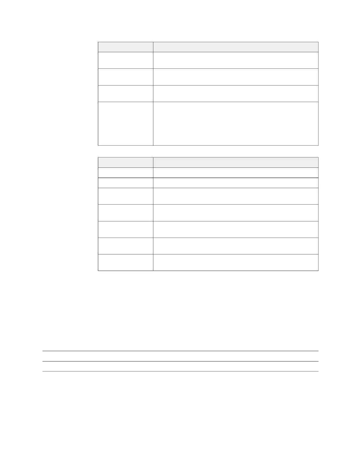
2. Add a PLL block with the following settings:
Option Description
Resource T13/T20 BGA169 and BGA256 only: Select BR_PLL0, which is the
only PLL the LVDS RX interface can use.
Reference
Clock Mode
External
Reference Clock
Frequency
Set the reference clock frequency to match the clock coming from
the LVDS RX reference clock you created in step 1.
Output Clock For LVDS deserializer widths 2 - 8, define the output clocks so that
you have one for the fast clock (serial) and one for the slow clock
(parallel).
Set the relationship between the clocks such that the serial clock
frequency = parallel clock frequency * (serialization / 2). The serial
clock must use the 90 degree phase shift.
3. Add an LVDS RX block with these settings:
Option Description
LVDS Type Receiver (RX)
LVDS Resource Any channel
Enable
Deserialization
On
Deserialization
Width
n
Output Pin/
Bus Name
Any
Serial Clock
Pin Name
Use the fast clock output name that corresponds to the PLL you
chose.
Parallel Clock
Pin Name
Use the slow clock output name that corresponds to the PLL you
chose.
4. Repeat step 3 for each LVDS RX data lane you want to implement.
Design Check: LVDS Errors and Warnings
When you check your design, the Interface Designer applies design rules to your LVDS
settings. The following tables show some of the error and warnng messages you may
encounter and explains how to fix them.
lvds_rule_bidir_tx (error)
Message Output enable pin name must be configured in Bidirectional LVDS Tx
To fix If you are using a bidirectional LVDS block, you need to specify the output enable pin name.
www.efinixinc.com 78