Titanium Interfaces User Guide
About the HSIO Interface
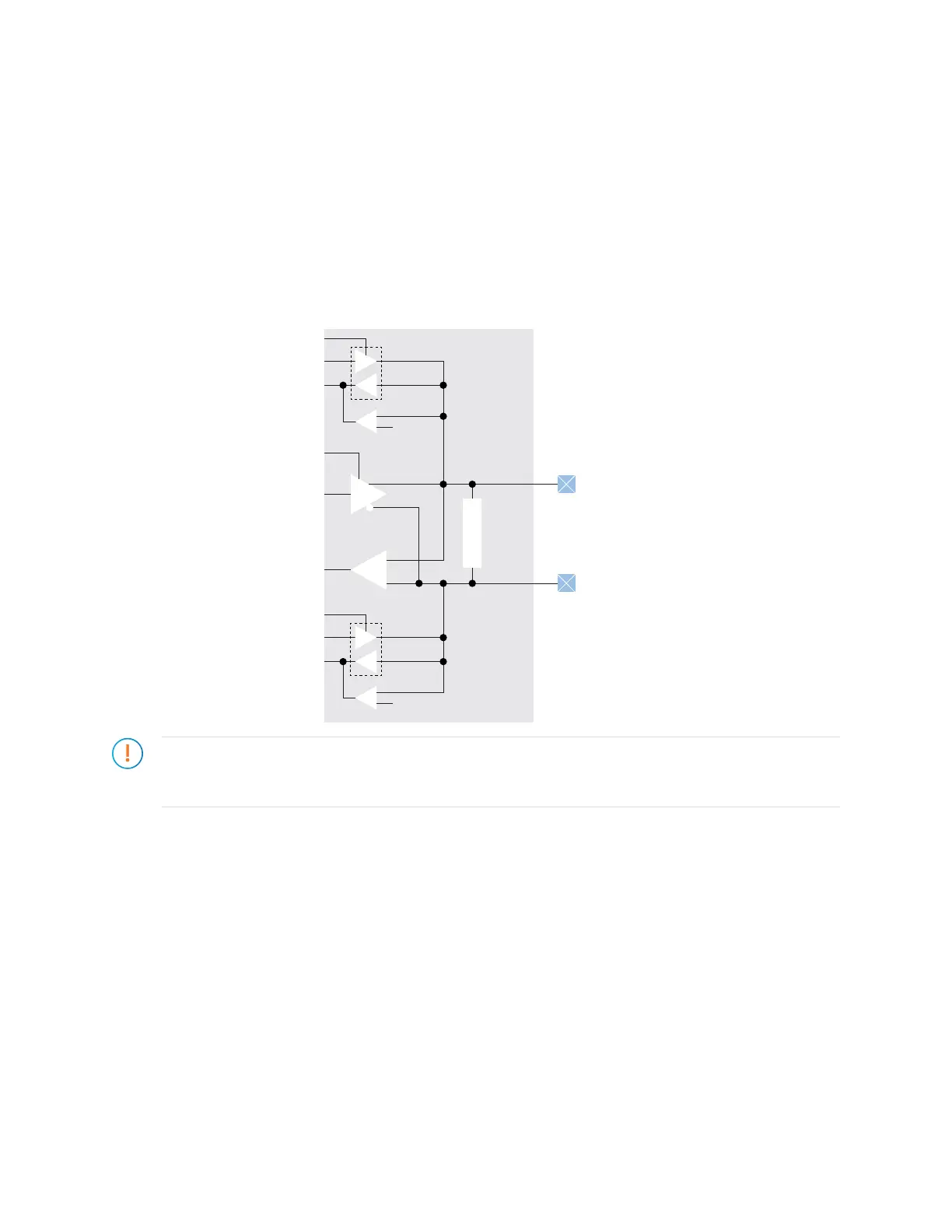
Each HSIO block uses a pair of I/O pins as one of the following:
• Single-ended HSIO—Two single-ended I/O pins (LVCMOS, SSTL, HSTL)
• Differential HSIO—One differential I/O pins:
— Differential SSTL and HSTL
— LVDS—Receiver (RX), transmitter (TX), or bidirectional (RX/TX)
— MIPI lane I/O—Receiver (RX) or transmitter (TX)
Figure 15: HSIO Buffer Block Diagram
Important: When you are using an HSIO pin as a GPIO, LVDS, or MIPI lanes, make sure to leave at least
1 pair of unassigned HSIO pins between the HSIO pins used as GPIO, LVDS, or MIPI lanes and HSIO pins.
This separation reduces noise. The Efinity software issues an error if you do not leave this separation.
www.efinixinc.com 46