Titanium Interfaces User Guide
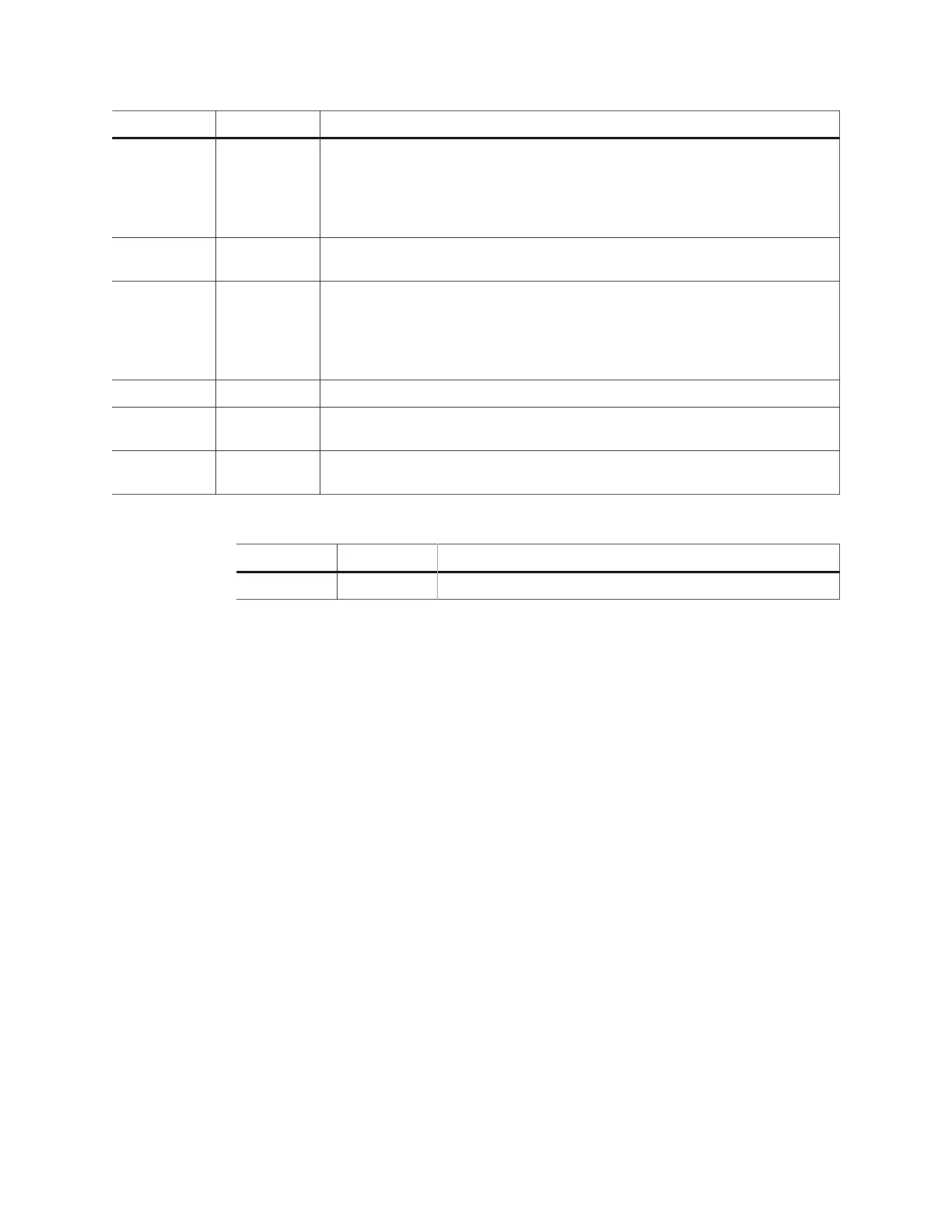
Table 31: HVIO Signals (Interface to FPGA Fabric)
Signal Direction Description
IN[1:0] Output Input data from the HVIO pad to the core fabric.
IN0 is the normal input to the core. In DDIO mode, IN0 is the data captured
on the positive clock edge (HI pin name in the Interface Designer) and IN1 is
the data captured on the negative clock edge (LO pin name in the Interface
Designer).
ALT Output Alternative input connection (in the Interface Designer, Register Option is
none). HVIO only support pll_clkin as the alternative connection.
OUT[1:0] Input Output data to HVIO pad from the core fabric.
OUT0 is the normal output from the core. In DDIO mode, OUT0 is the data
captured on the positive clock edge (HI pin name in the Interface Designer)
and OUT1 is the data captured on the negative clock edge (LO pin name in the
Interface Designer).
OE Input Output enable from core fabric to the I/O block. Can be registered.
OUTCLK Input Core clock that controls the output and OE registers. This clock is not visible in
the user netlist.
INCLK Input Core clock that controls the input registers. This clock is not visible in the user
netlist.
Table 32: HVIO Pads
Signal Direction Description
IO Bidirectional HVIO pad.
www.efinixinc.com 45