Titanium Interfaces User Guide
Design Considerations
• Because the TCK and TMS signals connect devices in the JTAG chain, they must have good
signal quality.
• TCK should transition monotonically at the receiving devices and should be terminated
correctly. Poor TCK quality can limit the maximum frequency you can use for
configuration.
• Buffer TMS and TCK so they have sufficient drive strength at all receiving devices.
• Ensure that the logic high voltage is compatible with all devices in the JTAG chain.
• If your chain contains devices from diffferent vendors, you might need to drive optional
JTAG signals, such as TRST and enables.
Timing Parameters
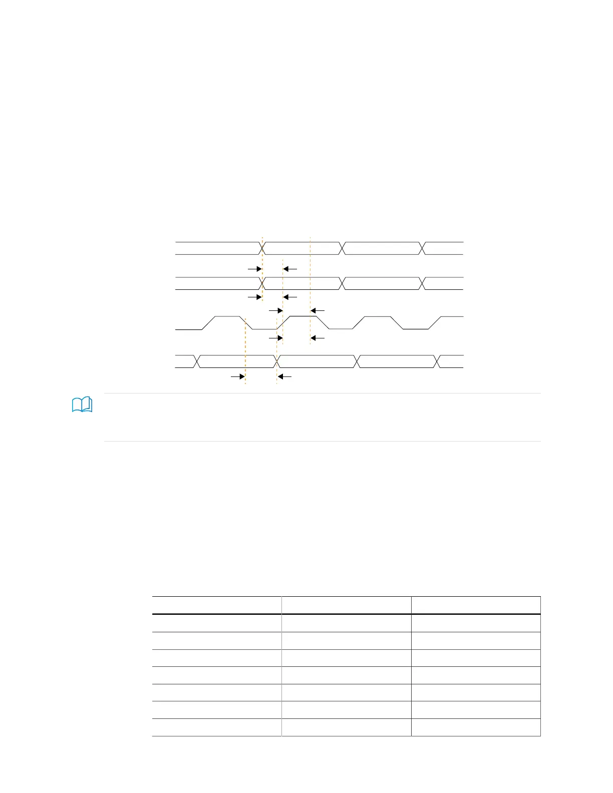
Figure 34: Boundary-Scan Timing Waveform
Learn more: Refer to the FPGA data sheet for timing specifications.
Refer to the Virtual I/O Debug Core section in the Efinity Software User Guide for more information about
JTAG User TAP interface.
Using the JTAG User TAP Block
Add the JTAG User TAP block to your interface if you want to use the FPGA JTAG pins to
communicate with the design running in the core.
You specify the instruction to use with the JTAG Resource setting. Titanium FPGAs have
four JTAG User TAP blocks. To use more than one, add JTAG User TAP blocks to your
interface design, one for each resource.
Table 48: JTAG User TAP Signals
Signal Direction Description
<instance>_TDI Input JTAG test data in pin.
<instance>_TCK Input JTAG test clock pin.
<instance>_TMS Input JTAG mode select pin.
<instance>_SEL Input User instructive active pin.
<instance>_DRCK Input Gated test clock.
<instance>_RESET Input REset.
<instance>_RUNTEST Input Run test pin.
www.efinixinc.com 92