Titanium Interfaces User Guide
1. Add a PLL block with the following settings:
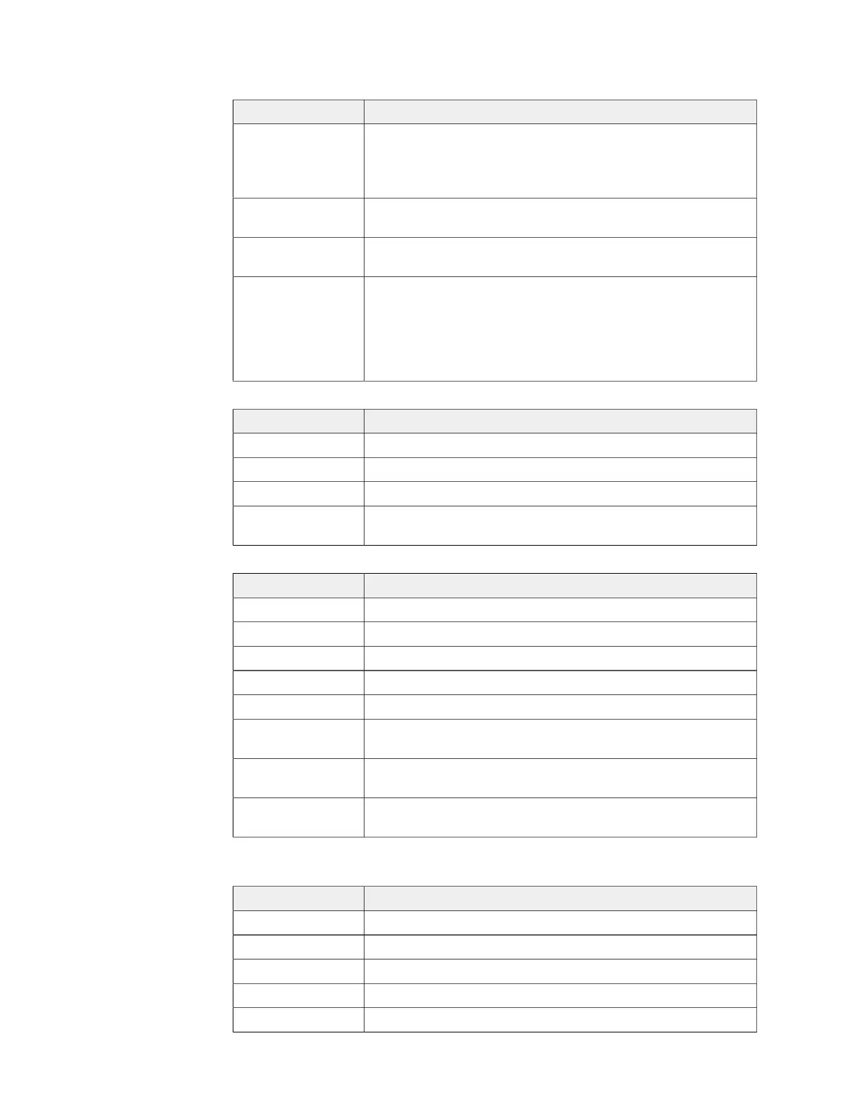
Option Description
Resource You can use any PLL resource.
T13/T20 BGA169 and BGA256 only: if you also want to create an
RX interface, do not select PLL_BR0 because it is the only PLL the
RX interface can use.
Reference
Clock Mode
External
Reference Clock
Frequency
Any
Output Clock For LVDS serializer widths 2 - 8, define the output clocks so that
you have one for the fast clock (serial) and one for the slow clock
(parallel).
Set the relationship between the clocks such that the serial clock
frequency = parallel clock frequency * (serialization / 2). The serial
clock must use the 90 degree phase shift.
2. Add a GPIO block with these settings to provide the reference clock input to the PLL:
Option Description
Mode Input
Pin Name Any
Connection Type pll_clkin
GPIO Resource Assign the dedicated PLL_CLKIN pin that corresponds to the PLL
you chose.
3. Add an LVDS TX block with these settings:
Option Description
LVDS Type Transmitter (TX)
LVDS Resource Any channel
Mode Serial data output
Enable Serialization On
Serialization Width n
Output Pin/
Bus Name
Any
Serial Clock
Pin Name
Use the fast clock output name that corresponds to the PLL you
chose.
Parallel Clock
Pin Name
Use the slow clock output name that corresponds to the PLL you
chose.
4. Repeat step 3 for each LVDS TX data lane you want to implement.
5. Add another LVDS block that will serve as the LVDS TX reference clock output:
Option Description
LVDS type Transmitter (TX)
LVDS resource Any channel
Mode Reference clock output
Enable Serialization On
Serialization width n
www.efinixinc.com 76