Titanium Interfaces User Guide
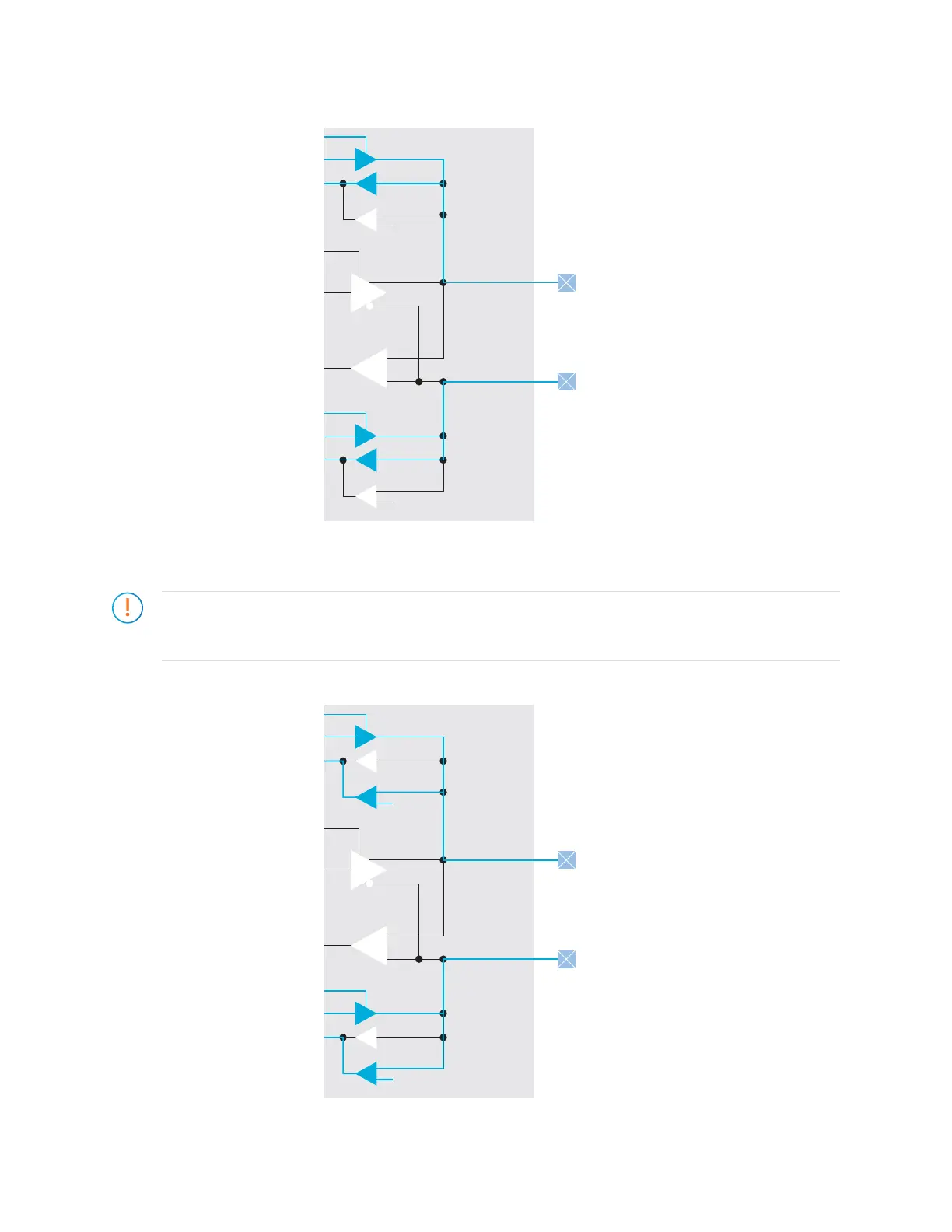
Figure 17: I/O Buffer Path for LVCMOS
When using an HSIO with the HSTL or SSTL I/O standards, you must configure an I/O pad
of the standard's input path as a VREF pin. There is one programmable VREF per I/O bank.
Important: When configuring an I/O pad of the standard's input path as a VREF pin, you must use the
VREF from the same physical I/O bank even when the I/O banks are merged to share a common VCCIO
pin.
Figure 18: I/O Buffer Path for HSTL and SSTL
www.efinixinc.com 49