Titanium Interfaces User Guide
The serial clock (also known as the fast clock) outputs data to the pin, the parallel clock (also
known as the slow clock) transfers it from the core. An equation defines the relationship
between the clocks. For LVDS TX the parallel clock captures data from the core and the
serial clock outputs it to the LVDS buffer.
In half-rate mode, new data is output on both edges of the serial clock, in full rate mode it is
only on the rising (positive) edge.
LVDS RX
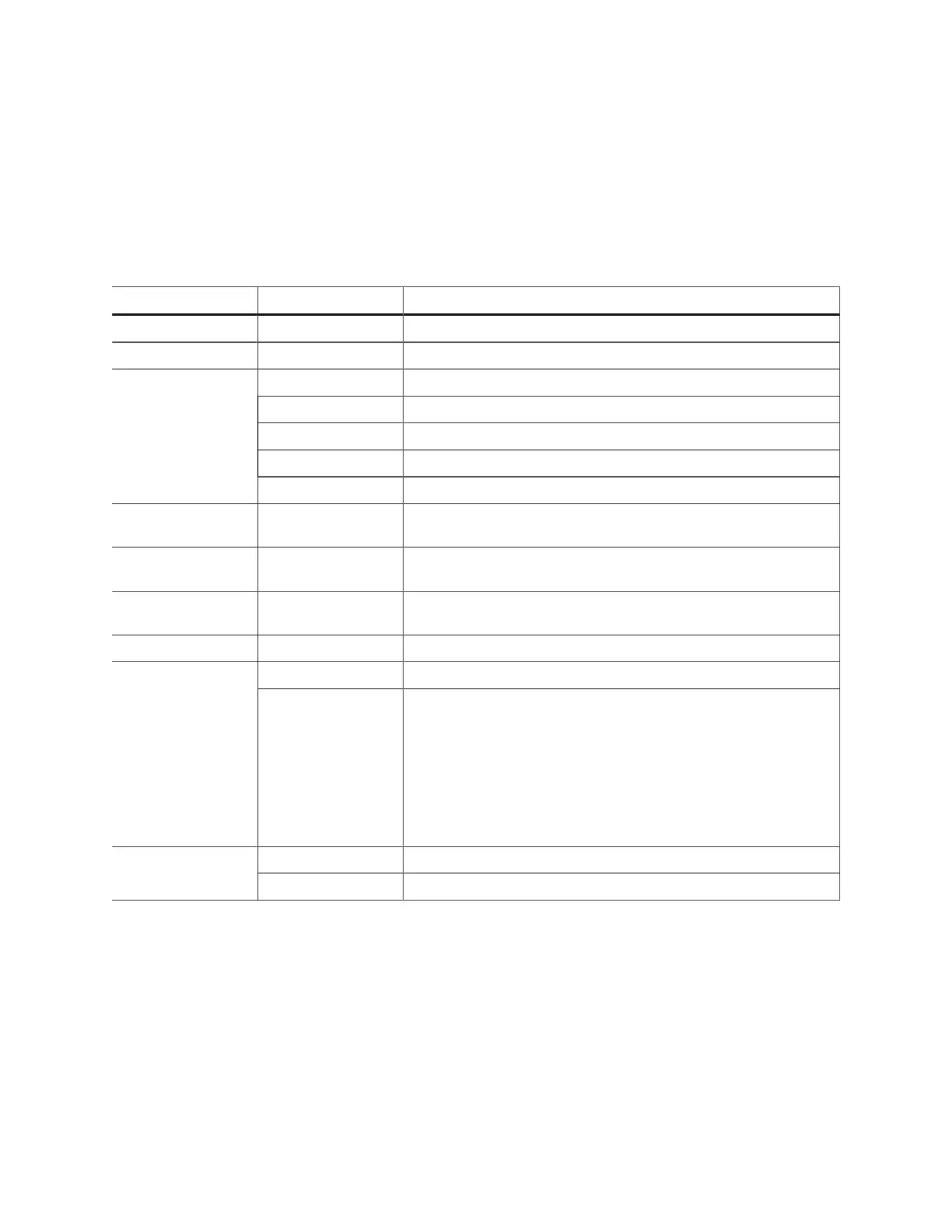
Table 43: LVDS RX Options
Option Choices Description
Instance Name User defined
LVDS Resource Resource list Choose a resource.
normal LVDS RX function.
pll_clkin Alternate function. Use as PLL reference clock.
pll_extfb Alternate function. Use as PLL external feedback.
gclk Alternate function. Use as global clock.
Connection Type
rclk Alternate function. Use as regional clock.
Input Pin/Bus Name User defined Input pin or bus that feeds the LVDS transmitter parallel data. The
width should match the deserialization factor.
Dynamic Enable Pin
Name
User defined Dynamically enables or disables the LVDS RX buffer. Disabling the
buffer can reduce power consumption when the pin is not in use.
Enable Common
Mode Driver
On or off If you implement an AC coupled connection, turn on tthis option.
For a typical DC coupled connection, leave this option off.
Termination on, off, dynamic For dynamic, specify the pin that controls the dynamic termination.
Off Use as a simple buffer.Enable
Deserialization
On Use as an LVDS deserializer:
• Optionally enable half rate serialization.
• Choose a width of 2, 3, 4, 5, 6, 7, 8, or 10 (1 is a simple buffer). A
width of 9 is not legal.
• Specify the serial clock and parallel clock.
• Optionally turn on Enable Clock Crossing FIFO, which uses
a FIFO to cross between the slow clock and the user core clock.
Specify the FIFO read, clock, and empty pin names.
static Integer from 0 - 63. Each step adds approximately 25 ps of delay.Delay Mode
dynamic Specify the pin names to control the dynamic delay.
The serial clock (also known as the fast clock) captures data from the pin, the parallel clock
(also known as the slow clock) transfers it to the core. An equation defines the relationship
between the clocks.
The maximum LVDS rate is 1.6 Gbps.
• Half rate
calculation—serial clock frequency = parallel clock frequency * (deserialization / 2)
• Full rate calculation—serial clock frequency = parallel clock * deserialization
The serial clock must have a phase shift that is between 45 and 135 degrees. Both clocks must
come from the same PLL.
www.efinixinc.com 74