EMBEDDED Intel486™ PROCESSOR HARDWARE REFERENCE MANUAL
7-8
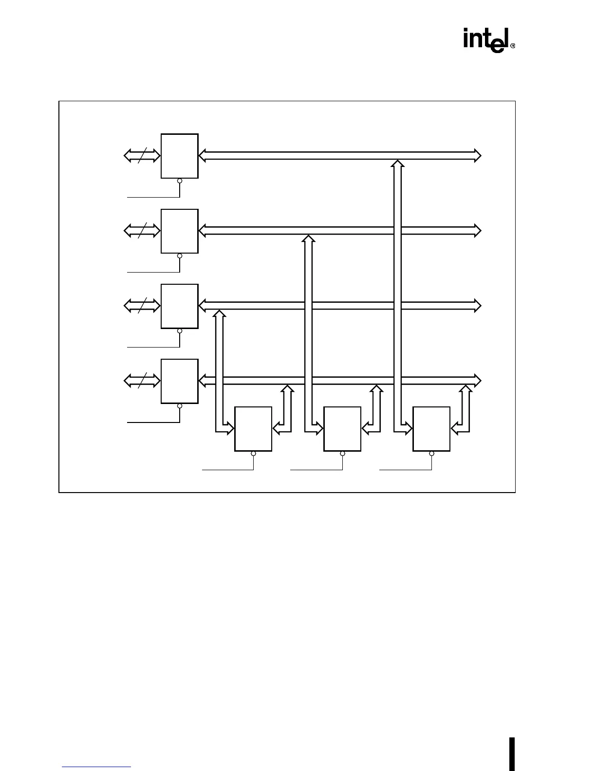
Figure 7-4. Intel486™ Processor Interface to 8-Bit Device
In this example of a 32-bit write, the BE3#–BE0# are enabled; hence 32 bits of data reside on the
data buffer outputs. This data is then swapped based on the control signals. Buffers are enabled
in the following manner:
For Byte # 0 Buffer 3 is enabled (BE0# is true)
For Byte # 1 Buffer 2 and 4 are enabled (BE1# and BEN8H#)
For Byte # 2 Buffer 1 and 5 are enabled (BE2# and BEN8UL#)
For Byte # 3 Buffer 0 and 6 are enabled (BE3# and BEN8UH#)
Table 7-5 shows the truth table for 8-bit I/O interface to the Intel486 processor. The table also
contains the values of the control signals used to enable the second set of buffers. The PLD equa-
tions used to implement these signals are shown in Tables 7-3 and 7-4.
A5283-02
BUFF
0
BEN8H#
4
BEN8UL#
5
8
BE3#
BEN8UH#
BUFF
1
8
BE2#
6
BUFF
2
8
BE1#
BUFF
3
8
BE0#
Bidirectional
Data Buffers
8-Bit
Bus
Intel486™
Processor
Interface