EasyManua.ls Logo

Intel Embedded Intel486 User Manual

Intel Embedded Intel486
334 pages
To Next Page IconTo Next Page
To Previous Page IconTo Previous Page
Page #215 background image
7-43
PERIPHERAL SUBSYSTEM
These similarities between the Intel486 processor and the 82596 coprocessor simplify bus arbi-
tration when the processor and the coprocessor are the only two bus masters on the processor bus.
The HOLD and HLDA signals can be used for handshake arbitration and BREQ from the proces-
sor can trigger the coprocessor’s bus throttle timers when needed, as shown in Figure 7-23.
Network (Serial) Interface
TxD
O Transmit data
TxC#
O Transmit clock
LPBK# O Loopback
RxD I Receive data
RxC# I Receive clock
RTS# O Request to send
CTS# I Clear to send
CRS# I Carrier sense
CDT# I Collision detect
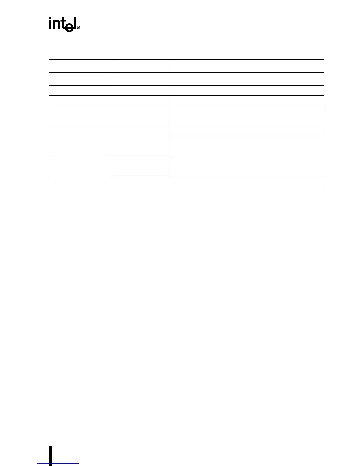
Table 7-12. 82596 Signals (Sheet 2 of 2)
Signal Type Description
Signals marked with a dagger are not included on, or operate differently than, the Intel486™ processor
bus.

Table of Contents

Question and Answer IconNeed help?

Do you have a question about the Intel Embedded Intel486 and is the answer not in the manual?

Intel Embedded Intel486 Specifications

General IconGeneral
BrandIntel
ModelEmbedded Intel486
CategoryComputer Hardware
LanguageEnglish

Summary

Introduction

Processor Features

Details core features like 32-bit RISC core, pipelining, on-chip cache, and MMU.

On-chip Cache

Details the 8/16-Kbyte unified cache, its protocols, and line fills.

Internal Architecture

Instruction Pipelining

Explains how instructions are processed in stages for improved performance.

Cache Unit

Covers cache operation, including hits, misses, line fills, and update policies.

Bus Operation

Data Transfer Mechanism

Explains how data operands of various lengths are transferred over the bus.

Locked Cycles

Covers atomic memory access using the LOCK# pin for read-modify-write operations.

Memory Subsystem Design

Improving Write Cycle Latency

Covers techniques like interleaving and write posting to reduce write latency.

Second-Level Cache

Explains the advantages and performance benefits of using an L2 cache.

Peripheral Subsystem

System Bus Design

PCI BUS: SYSTEM DESIGN EXAMPLE

Introduces the PCI bus, its features, and its implementation in embedded systems.

Performance Considerations

Instruction Execution Performance

Reviews how Intel486 processors achieve faster instruction execution and compares with earlier processors.

Internal Cache Performance Issues

Analyzes the on-chip cache's organization, size, and impact on performance.

On-Chip Write Buffers

Details the function of write buffers in reducing latency and enhancing write performance.

Second-Level Cache Performance Considerations

Explains the advantages and performance benefits of using an L2 cache.

Floating-Point Performance

Analyzes the floating-point unit's performance, execution sequences, and on-chip interface.

Physical Design and System Debugging

Power Dissipation and Distribution

Discusses power dissipation, capacitive loading, and power/ground planes.

High-Frequency Design Considerations

Covers management of transmission lines, impedance control, and EMI.

Latch-Up

Covers prevention of latch-up by observing voltage limits and using proper layout.

Clock Considerations

Discusses requirements for clock signals, skew, and loading effects.

Thermal Characteristics

Explains thermal specifications, junction temperature calculation, and heatsink usage.

Building and Debugging the Intel486™ Processor-Based System

Outlines steps for building and debugging the system incrementally.

Related product manuals