EMBEDDED Intel486™ PROCESSOR HARDWARE REFERENCE MANUAL
3-4
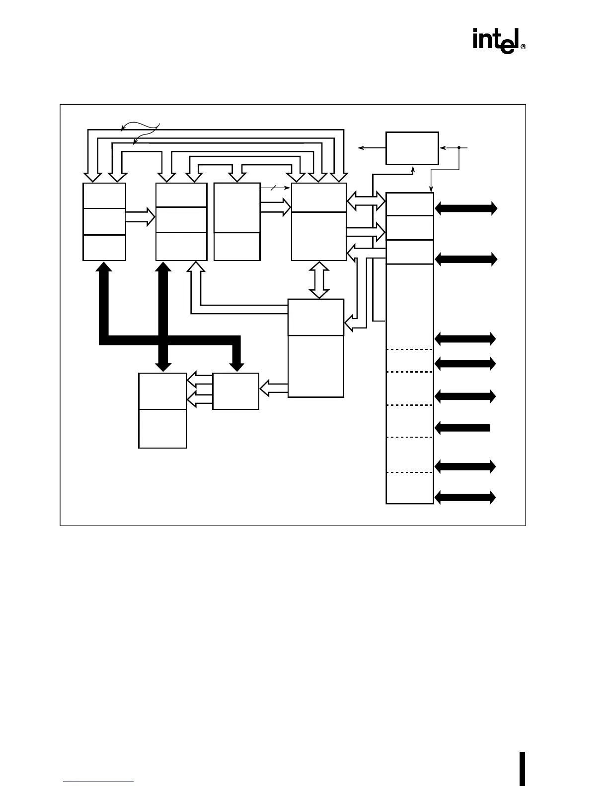
Figure 3-3. Ultra-Low Power Intel486™ SX and Ultra-Low Power Intel486 GX Processors
Block Diagram
Signals from the external 32-bit processor bus reach the internal units through the bus interface
unit. On the internal side, the bus interface unit and cache unit pass addresses bi-directionally
through a 32-bit bus. Data is passed from the cache to the bus interface unit on a 32-bit data bus.
The closely coupled cache and instruction prefetch units simultaneously receive instruction
prefetches from the bus interface unit over a shared 32-bit data bus, which the cache also uses to
receive operands and other types of data. Instructions in the cache are accessible to the instruction
prefetch unit, which contains a 32-byte queue of instructions waiting to be executed.
The on-chip cache is 16 Kbytes for the IntelDX4 processor and 8 Kbytes for all other members
of the Intel486 processor family. It is 4-way set associative and follows a write-through policy.
The Write-Back Enhanced IntelDX4 processor can be set to use an on-chip write-back cache pol-
Paging
Unit
Prefetcher
32-Byte Code
Queue
2x16 Bytes
Code
Stream
Barrel
Shifter
24
Cache Unit
Burst Bus
Control
Bus Control
Write Buffers
4 x 32
64-Bit Interunit Transfer Bus
Register
File
ALU
Segmentation
Unit
Descriptor
Registers
Limit and
Attribute PLA
32
Base/
Index
Bus
Translation
Lookaside
Buffer
20
8 Kbyte
Cache
Clock
Control
Control &
Protection
Test Unit
Control
ROM
Address
Drivers
CLK
Core
Clock
32
32
Data Bus
Transceivers
32
Request
Sequencer
Bus Size
Control (on
ULP486 SX
only)
Cache
Control
Parity
Generation
and Control
Boundary
Scan
Control
Bus Interface
D31-D0 on ULP486™ SX
D15-D0 on ULP486™ GX
A31-A2
BE3#- BE0#
ADS# W/R# D/C# M/IO#
PCD PWT RDY# LOCK#
PLOCK# BOFF# A20M#
BREQ HOLD HLDA
RESET SRESET INTR
NMI SMI# SMIACT#
FERR# IGNNE#
STPCLK#
A5440-01
BRDY# BLAST#
BS16# BS8# (not present
on ULP486 GX)
KEN# FLUSH#
AHOLD EADS#
DP3-DP0 PCHK# on
ULP486 SX
DP1-DP0 PCHK# on
ULP486 GX
TCK TMS
TDI TD0
128
Instruction
Decode
32
Decoded
Instruction
Path
PCD
PWT
2
Physical
Address
32-Bit Data Bus
32-Bit Data Bus
Linear Address
Micro-
Instruction
Displacement Bus
32