MOTOROLA M68020 USER’S MANUAL 5- 33
5.3.2 Write Cycle
During a write cycle, the processor transfers data to memory or a peripheral device.
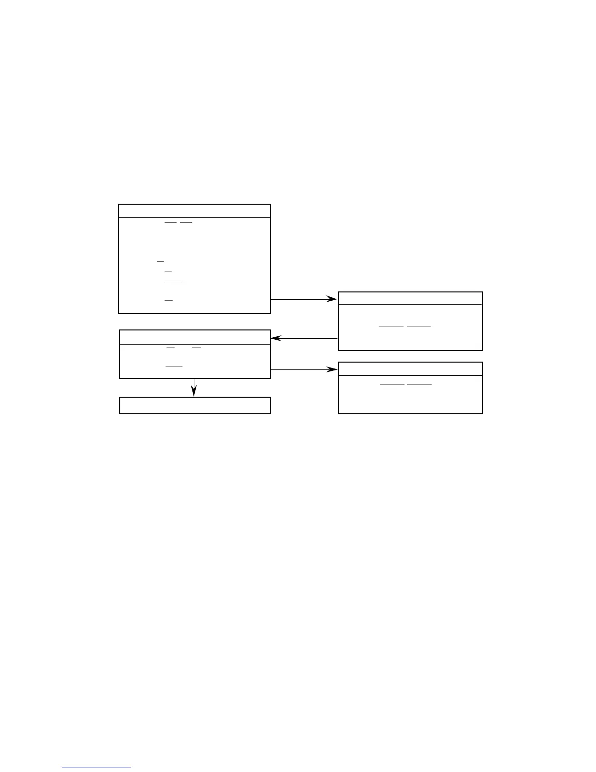
Figure 5-24 is a flowchart of a write cycle operation for a long-word transfer. Figures 5-25–
5-28 are write cycle timing diagrams in terms of clock periods. Figure 5-25 shows two
write cycles (between two read cycles with no idle time in between) for a 32-bit port.
Figure 5-26 shows byte and word write cycles to a 32-bit port. Figure 5-27 shows a long-
word write cycle to an 8-bit port. Figure 5-28 shows a long-word write cycle to a 16-bit
port.
1) ASSERT ECS/OCS FOR ONE-HALF CLOCK
2
) DRIVE ADDRESS ON A31–A0
) DRIVE FUNCTION CODES ON FC2–FC0
) DRIVE SIZ1, SIZ0 (FOUR BYTES)
) SET R/W TO WRITE
) ASSERT AS
) ASSERT DBEN
) DRIVE DATA LINES D31–D0
) ASSERT DS
) REMOVE DATA FROM D31–D0
) NEGATE DBEN
) STORE DATA FROM D31–D0
) ASSERT DSACK1/DSACK0
TERMINATE OUTPUT TRANSFER
This step does not apply to the MC68EC020.
For the MC68EC020, A23–A0.
Figure 5-24. Write Cycle Flowchart

 Loading...
