9- 12 M68020 USER’S MANUAL MOTOROLA
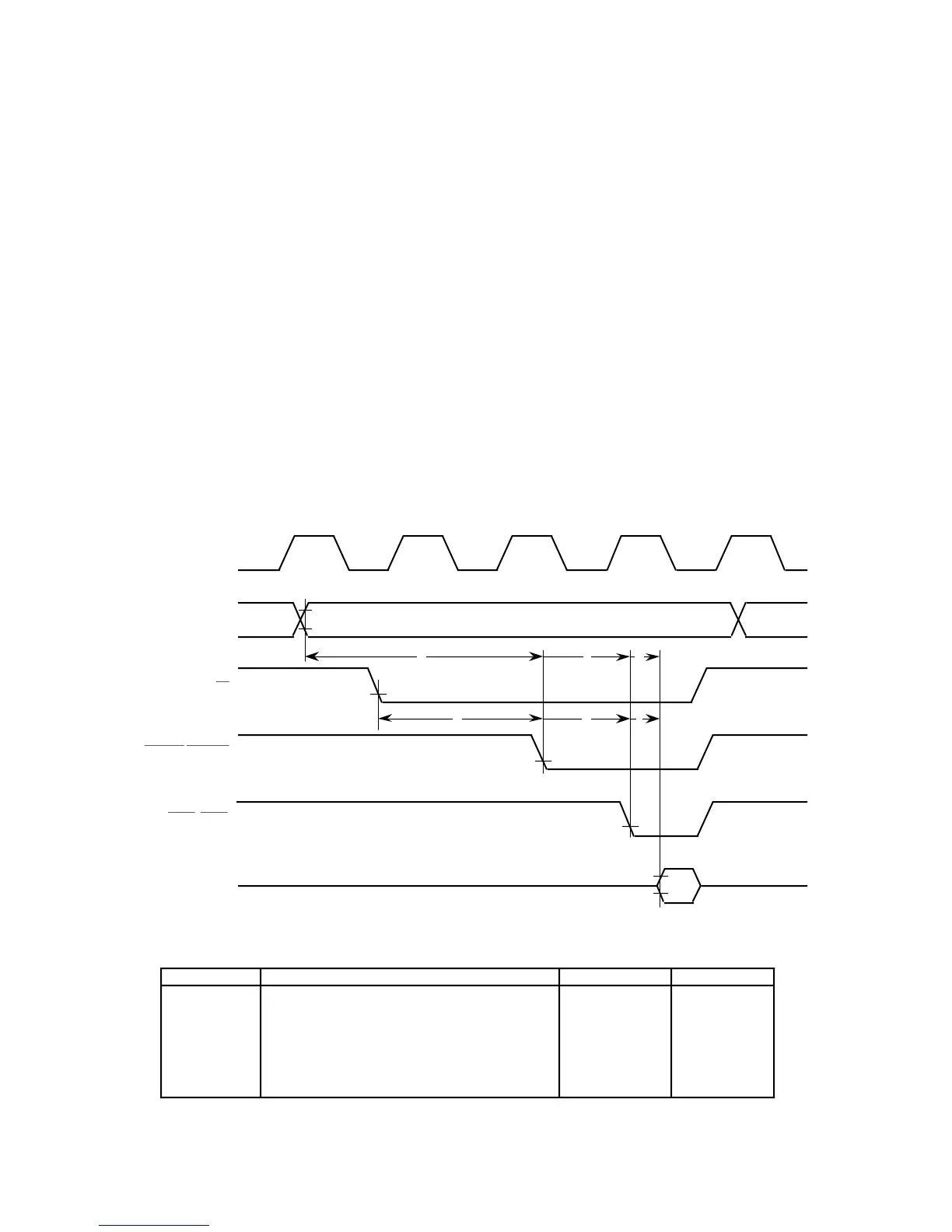
9.6 ACCESS TIME CALCULATIONS
The timing paths that are critical in any memory interface are illustrated and defined in
Figure 9-9.
The type of device that is interfaced to the MC68020/EC020 determines exactly which of
the paths is most critical. The address-to-data paths are typically the critical paths for
static devices since there is no penalty for initiating a cycle to these devices and later
validating that access with the appropriate bus control signal. Conversely, the address-
strobe-to-data-valid path is often most critical for dynamic devices since the cycle must be
validated before an access can be initiated. For devices that signal termination of a bus
cycle before data is validated (e.g., error detection and correction hardware and some
external caches), to improve performance, the critical path may be from the address or
strobes to the assertion of
BERR (or BERR and HALT). Finally, the address-valid-to-
DSACK1/DSACK0-asserted path is most critical for very fast devices and external
caches, since the time available between the address becoming valid and the
DSACK1/DSACK0 assertion to terminate the bus cycle is minimal. Table 9-4 provides
the equations required to calculate the various memory access times assuming a 50-
percent duty cycle clock.
NOTE: This diagram illustrates access time calculations only
For the MC68EC020, A23–A0.
Parameter Description System Equation
a
Address Valid to DSACK1/DSACK0 Asserted
t
AVDL
9-3
b
AS Asserted to DSACK1/DSACK0 Asserted
t
SADL
9-4
c
Address Valid to BERR/HALT Asserted
t
AVBHL
9-5
d
AS Asserted to BERR/HALT Asserted
t
SABHL
9-6
e Address Valid to Data Valid t
AVDV
9-7
f
AS Asserted to Data Valid
t
SADV
9-8

 Loading...
