13-8 MC68838 USER’S MANUAL MOTOROLA
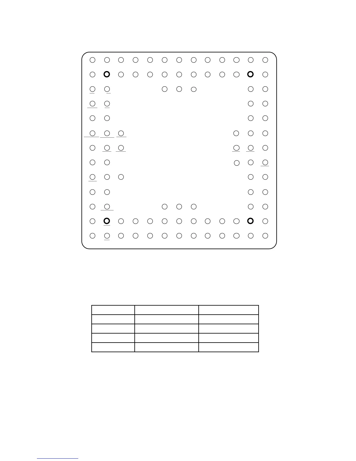
11.2.7 MC68EC020 RP Suffix—Pin Assignment
The V
CC
and GND pins are separated into four groups to provide individual power supply
connections for the address bus buffers, data bus buffers, and all other output buffers and
internal logic. It is recommended that all pins be connected to power and ground as
indicated.
Group V
CC
GND
Address Bus B7, C7 A1, A7, C8, D13
Data Bus K12, M9, N9 J13, L8, M1, M8
Logic D1, D2, E12, E13 F11, F12, J1, J2
Clock — B1

 Loading...
