13-10 MC68838 USER’S MANUAL MOTOROLA
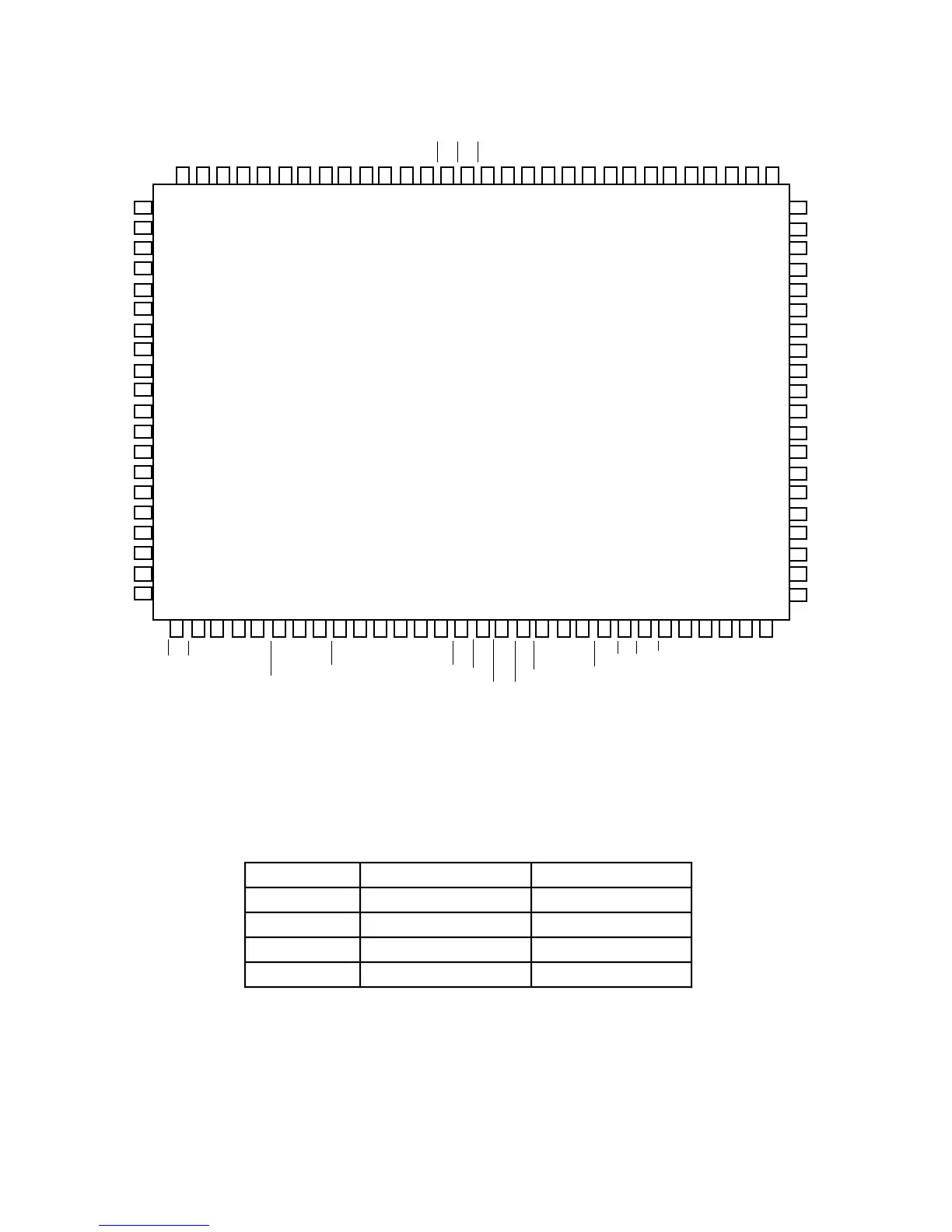
11.2.9 MC68EC020 FG Suffix—Pin Assignment
BR
BG
A8*
CLK
RESET
GND
GND
RMC
FC0
FC1
FC2
SIZ0
SIZ1
CDIS
AVEC
DSACK0
DSACK1
BERR
D7
D8
HALT
AS
DS
R/W
D31
D30
D29
D28
D9
V
CC
GND
V
CC
D6
D5
GND
D4
D3
D2
D1
D0
IPL0
IPL1
IPL2
GND
GND
GND
A2
A3
A4
A5
A6
A7
V
CC
V
CC
(TOP VIEW
NC*
NC
V
CC
GND
GND
GND
*NC—Do not connect to this pin.
The V
CC
and GND pins are separated into four groups to provide individual power supply
connections for the address bus buffers, data bus buffers, and all other output buffers and
internal logic. It is recommended that all pins be connected to power and ground as
indicated. NC pins are reserved by Motorola for future use and should have no external
connection.
Group V
CC
GND
Address Bus 90 72, 89, 100
Data Bus 44, 57 26, 43, 58, 59
Logic 7, 8, 70, 71 3, 20, 21, 68, 69
Clock — 4

 Loading...
