MOTOROLA MC68838 USER’S MANUAL 13-5
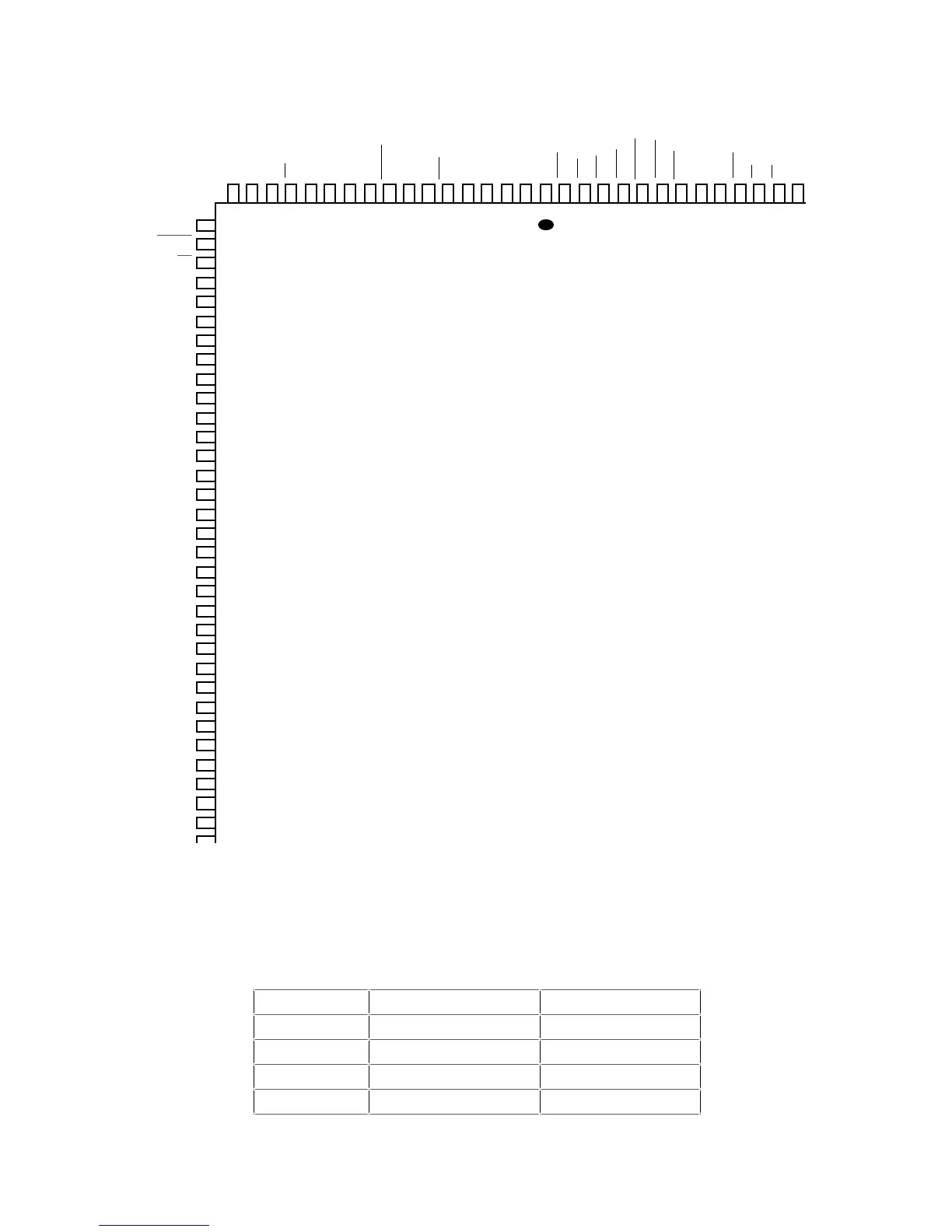
11.2.4 MC68020 FC and FE Suffix—Pin Assignment
VCC
67
NC*
NC*
NC*
A9
A8
A7
A6
A5
A4
A3
A2
GND
GND
GND
D0
D1
D2
D3
D4
GND
GND
D5
NC*
NC*
V
CC
V
CC
V
CC
VCC
NC*
NC*
GND
BG
GND
GND
CLK
RESET
V
CC
V
CC
RMC
FC0
FC1
FC2
SIZ0
SIZ1
DBEN
ECS
CDIS
AVEC
DSACK0
DSACK1
BERR
GND
GND
HALT
AS
R/W
NC*
DS
GND
GND
IPEND
OCS
IPL2
IPL1
IPL0
The V
CC
and GND pins are separated into four groups to provide individual power supply
connections for the address bus buffers, data bus buffers, and all other output buffers and
internal logic. It is recommended that all pins be connected to power and ground as
indicated. NC pins are reserved by Motorola for future use and should have no external
connection.
Group V
CC
GND
Address Bus 13, 38, 39 15, 40, 41, 62
Data Bus 79, 80, 96, 97 77, 78, 98, 99, 119, 120
Logic 7, 8, 65, 66 67, 68, 124, 125
Clock — 11, 12

 Loading...
