9- 14 M68020 USER’S MANUAL MOTOROLA
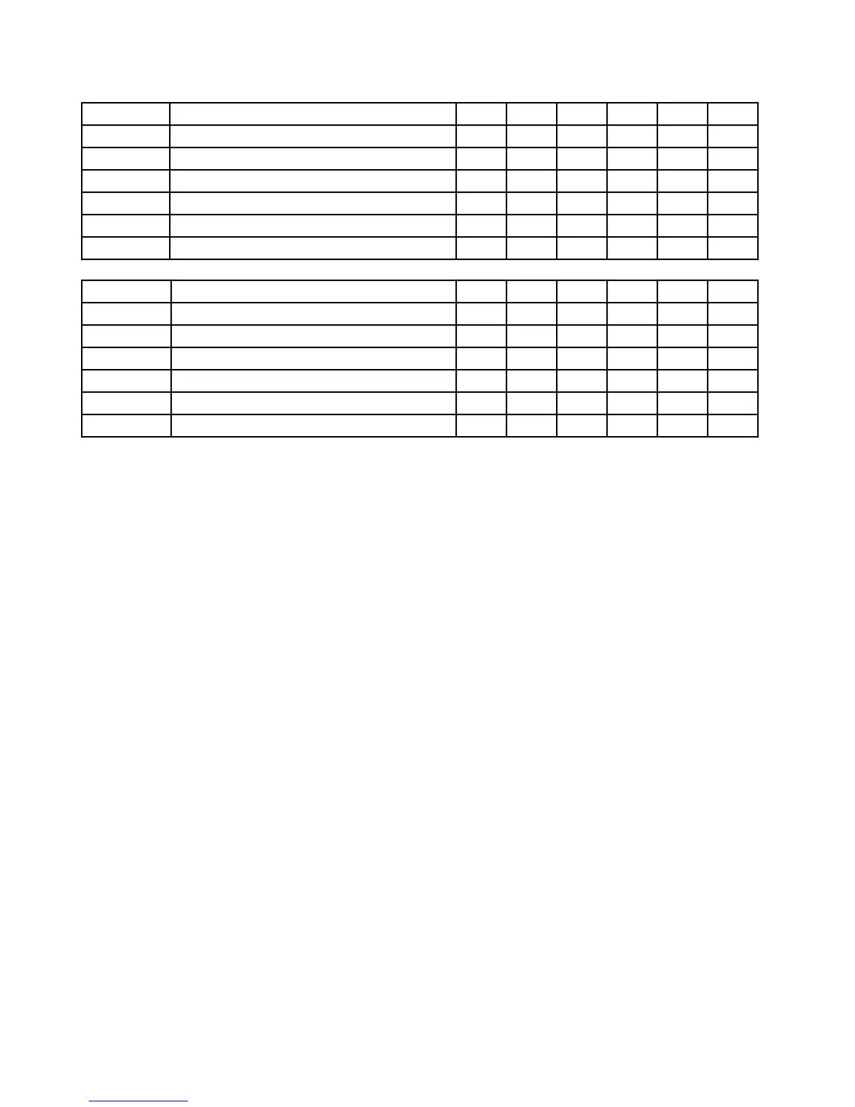
Table 9-4. Memory Access Time Equations at 16.67 and 25 MHz
Equation 16.667 MHz N = 3 N = 4 N = 5 N = 6 N = 7 Unit
9-3 t
AVDL
= (N – 1) • t1 – t2 – t6 – t47A 61 121 181 241 301 ns
9-4 t
SADL
= (N – 1) • t1 – t9 – t60 25 85 145 205 265 ns
9-5 t
AVBHL
= N • t1 – t2 – t6 – t27A 22 46 70 94 118 ns
9-6 t
SABHL
= (N – 1) • t1 – t9 – t27A 40 70 100 130 160 ns
9-7 t
AVDV
= N • t1 – t2 – t6 – t27 121 181 241 301 361 ns
9-8 t
SADV
= (N – 1) • t1 – t9 – t27 85 145 205 265 325 ns
Equation 25 MHz N = 3 N = 4 N = 5 N = 6 N = 7 Unit
9-3 t
AVDL
= (N – 1) • t1 – t2 – t6 – t47A 31 71 111 151 191 ns
9-4 t
SADL
= (N – 1) • t1 – t9 – t60 17 57 97 137 177 ns
9-5 t
AVBHL
= N • t1 – t2 – t6 – t27A 22 41 60 79 98 ns
9-6 t
SABHL
= (N – 1) • t1 – t9 – t27A 26 44 62 80 98 ns
9-7 t
AVDV
= N • t1 – t2 – t6 – t27 71 111 151 191 231 ns
9-8 t
SADV
= (N – 1) • t1 – t9 – t27 57 97 137 177 217 ns
Where:
tX = Refers to AC Electrical Specification X
t1 = The Clock Period
t2 = The Clock Low Time
t3 = The Clock High Time
t6 = The Clock High to Address Valid Time
t9 = The Clock Low to
AS Low Delay
t27 = The Data-In to Clock Low Setup Time
t27A = The
BERR/HALT to Clock Low Setup Time
t47A = The Asynchronous Input Setup Time
N = The Total Number of Clock Periods in the Bus Cycle (N ≥ 3 Cycles)
During asynchronous bus cycles, DSACK1/DSACK0 are used to terminate the current
bus cycle. In true asynchronous operations, such as accesses to peripherals operating at
a different clock frequency, either or both signals may be asserted without regard to the
clock, and then data must be valid a certain amount of time later as defined by
specification 31. With a 25-MHz controller, this time is 32 ns after
DSACK1/DSACK0
asserts; with a 16.67-MHz controller, this time is 50 ns after DSACK1/DSACK0 asserts
(both numbers vary with the actual clock frequency).
However, many local memory systems do not operate in a truly asynchronous manner
because either the memory control logic can be related to the MC68020/EC020 clock or
worst-case propagation delays are known; thus, asynchronous setup times for the
DSACK1/DSACK0 signals can be guaranteed. The timing requirements for this pseudo-
synchronous
DSACK1/DSACK0 generation is governed by the equation for t
AVDL
.

 Loading...
