5- 2 M68020 USER’S MANUAL MOTOROLA
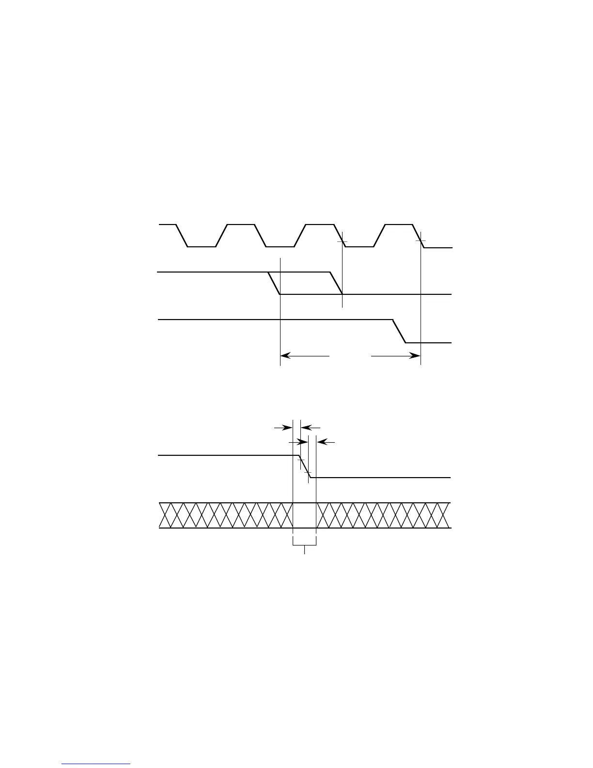
input is high or low. Figure 5-1 shows the relationship between the clock signal, a typical
input, and its associated internal signal.
Furthermore, for all inputs, the processor latches the level of the input during a sample
window around the falling edge of the clock signal. This window is illustrated in Figure 5-2.
To ensure that an input signal is recognized on a specific falling edge of the clock, that
input must be stable during the sample window. If an input transitions during the window,
the level recognized by the processor is not predictable; however, the processor always
resolves the latched level to either a logic high or logic low before using it. In addition to
meeting input setup and hold times for deterministic operation, all input signals must obey
the protocols described in this section.
Figure 5-1. Relationship between External and Internal Signals
INDOW
Figure 5-2. Input Sample Window
5.1.1 Bus Control Signals
The MC68020/EC020 initiates a bus cycle by driving the A1–A0, SIZ1, SIZ0, FC2–FC0,
and R/W outputs. However, if the MC68020/EC020 finds the required instruction in the on-
chip cache, the processor aborts the cycle before asserting the AS.The assertion of AS
ensures that the cycle has not been aborted by these internal conditions.

 Loading...
