RL78/F13, F14 CHAPTER 8 TIMER RD
R01UH0368EJ0210 Rev.2.10 653
Dec 10, 2015
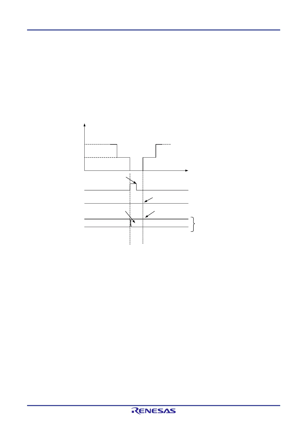
The TRD1 register counts 1, 0, FFFFH, 0, 1, in that order, when changing from decrement to increment operation.
Counting from 1, to 0, to FFFFH causes the UDF bit in the TRDSRi register to be set to 1. Also, when bits CMD1 and
CMD0 in the TRDFCR register are set to 10B (complementary PWM mode, buffer data transferred at underflow of the
TRD1 register), the content of the buffer registers (TRDGRD0, TRDGRC1, and TRDGRD1) is transferred to the general
registers (TRDGRB0, TRDGRA1, and TRDGRB1).
During operation of FFFFH, 0, and 1, data is not transferred to registers such as the TRDGRB0 register.
Also, at this time, the OVF bit in the TRDSRi register remains unchanged.
Figure 8-64. Operation When TRD1 Register Underflows in Complementary PWM Mode
1
0
FFFFH
0
Count value in
TRD1 register
UDF bit in
TRDSR1 register
OVF bit in
TRDSR1 register
TRDGRB0 register
Not transferred from buffer
register
No change
Time
When bits CMD1 and CMD0 in the
TRDFCR register are set to 10B
(transfer from the buffer register to the
general register when the TRD1 registe
underflows).
Transferred from
buffer register
Set to 0 by a program
TRDGRA1register
TRDGRB1register
 Loading...


