RL78/F13, F14 CHAPTER 8 TIMER RD
R01UH0368EJ0210 Rev.2.10 654
Dec 10, 2015
The timing of data transfer from the buffer register to the general register should be selected using bits CMD0 and
CMD1 in the TRDFCR register. However, regardless of the values of bits CMD0 and CMD1, transfer takes place
with the following timing when duty cycle is 0% and duty cycle is 100%.
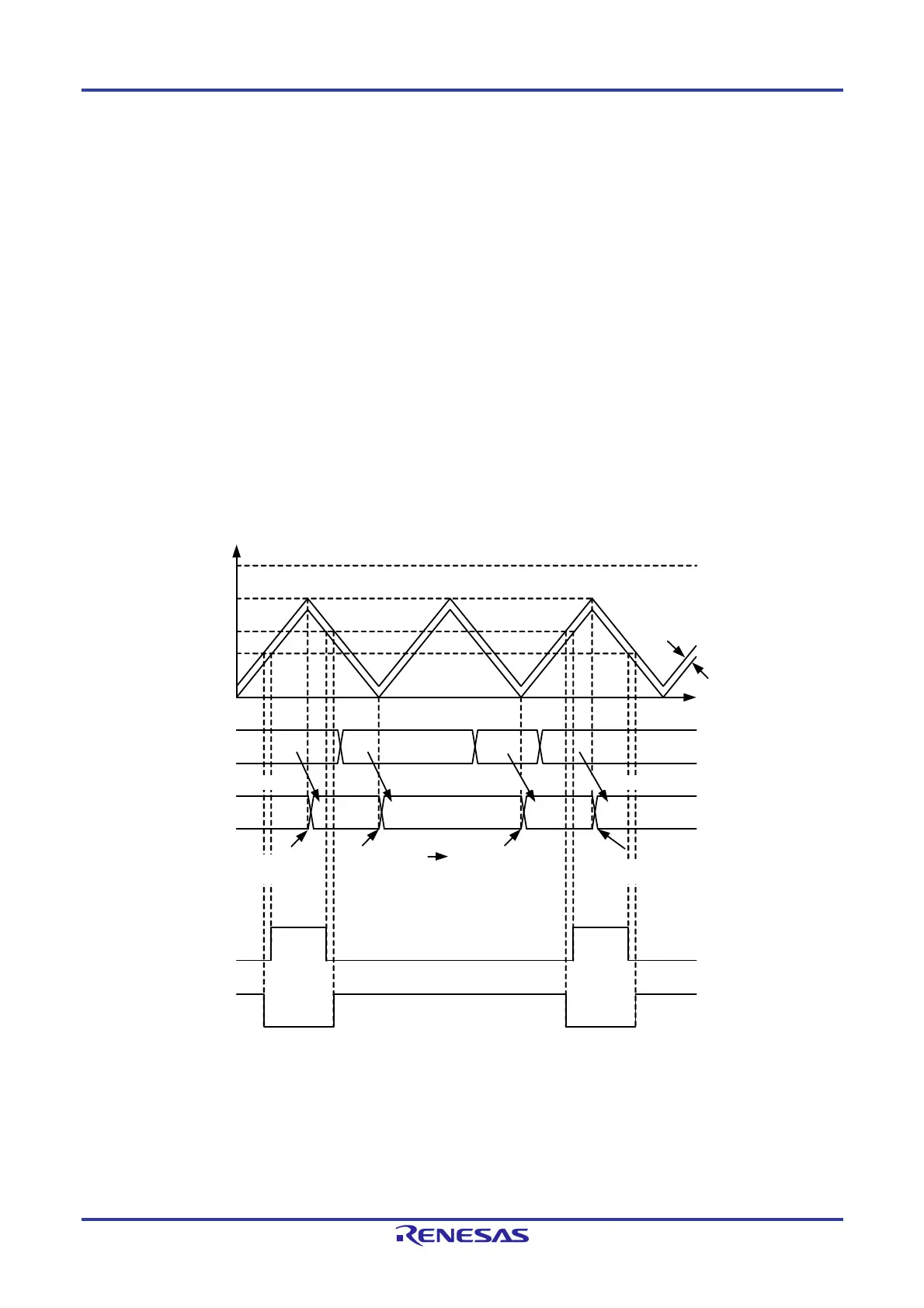
Value in buffer register value in TRDGRA0 register (duty cycle is 0%):
Transfer take place at underflow of the TRD1 register.
After this, when the buffer register is set to 0001H or above and a smaller value than the value of the TRDGRA0
register, and the TRD1 register underflows for the first time after setting, the value is transferred to the general
register. After that, the value is transferred with the timing selected by bits CMD1 and CMD0. A direct change of
the duty from 0% to 100% is not possible.
However, no waveform with duty cycle 0% can be generated while the initial value of the buffer register is FFFFH.
To generate a waveform with duty cycle 0%, set the value of the buffer register TRDGRA0 by writing to the
buffer register.
Figure 8-65. Operation When Value in Buffer Register Value in TRDGRA0 Register in Complementary
PWM Mode
n3
m+1
n2
n1
0000H
2n3n2n
n2 n3 n2 1n1n
n1
Value in
TRDi register
TRDGRD0 register
TRDGRB0 register
TRDIOB0 output
TRDIOD0 output
Transfer with timing set by
bits CMD1 and CMD0
Remark
m: Value set in TRDGRA0 register
Transfer at
underflow of
TRD1 register
because of n3 >
m
Transfer at
underflow of TRD1
register because
of first setting to
n2 < m
Transfer with timing set by
bits CMD1 and CMD0
Transfer
Count value in TRD1
Time
Count value in TRD0
TransferTransferTransfer
The above diagram applies under the following conditions :
• Bits CMD1 and CMD0 in the TRDFCR register are set to 11B
(data in the buffer register is transferred at compare match between registers TRD 0 and TRDGRA0 in complementary
PWM mode).
• Both the OSL0 and OLS1 bits in the TRDFCR register are set to 1 (active high for normal-phase and counter-phase).
 Loading...


