• Parasitic oscillation of outputs
• Modication of characteristic values (e.g. input/output voltage of analog devices)
4.4.2.4 Internal signal routing
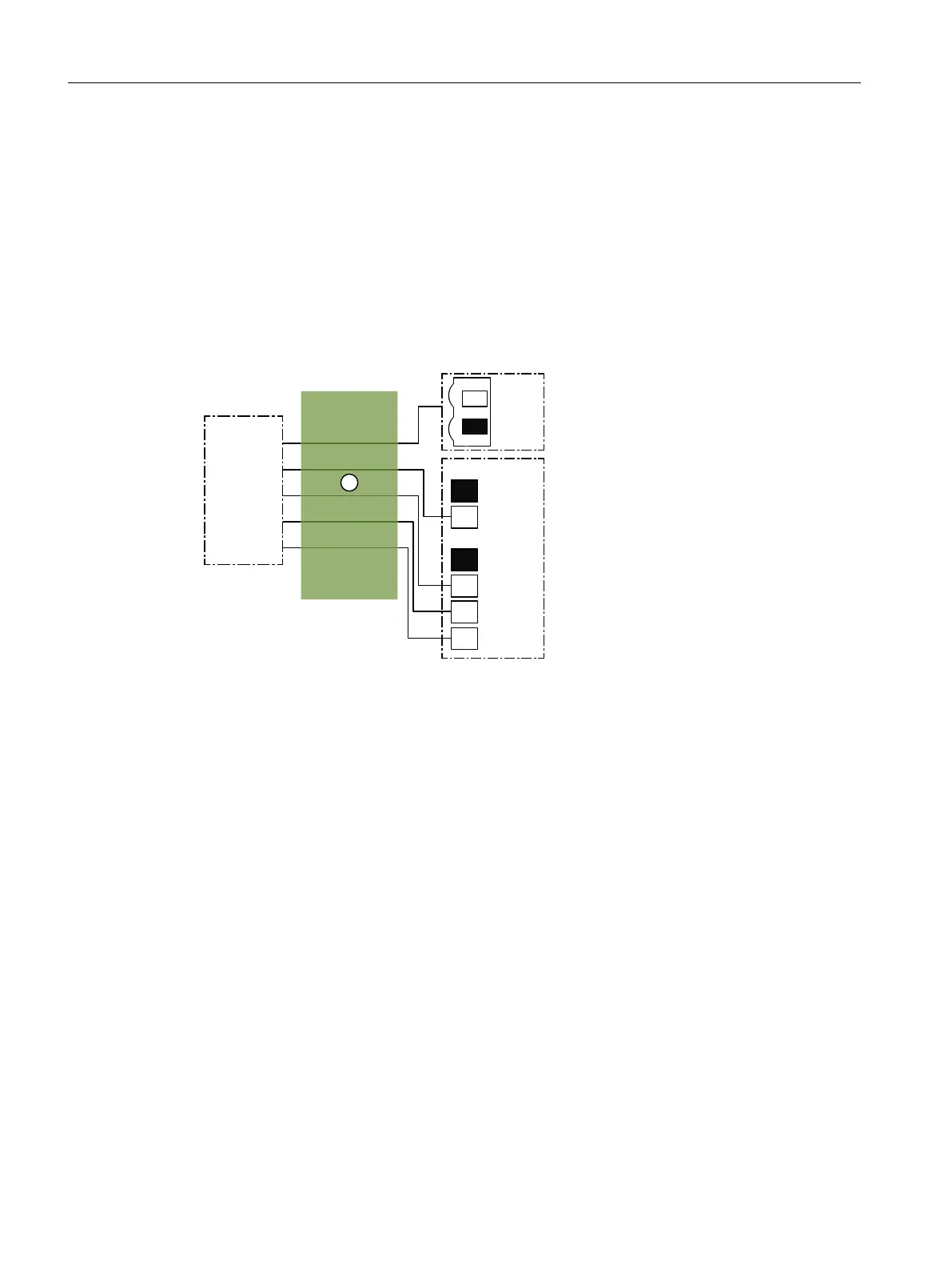
The following gure illustrates the input terminals and the internal wiring to the processor. The
input signals are located at processor port M. Separate reference potentials 0M, 1M and 2M can
each be dened for Input 2, Input 3, Input 4 and for Input 1 and Input 0. The input signals are
provided with internal pull-ups and there are no components between the input terminals and
the processor that are capable of oscillation.
,1387
,1387
,1
,1387
,1
,1387
,1
0
,1387
,1
0
;
,1
0
;
30
30
30
3257
30
30
① No components capable of oscillation and internal pull-up circuit
0M Ground potential 1
1M Ground potential 2
2M Ground potential 3
Figure 4-11 Internal wiring of input terminals
4.4.2.5 Redundant antivalent signal logic with discrepancy analysis
In the case of 1oo2 evaluation, the sensor is routed to two dierent, mutually antivalent
channels and is therefore evaluated by the controller twice. The discrepancy analysis is
performed between the two channels of the 1oo2 evaluation in the controller. If there is a
discrepancy between the input signals after expiry of the parameterized discrepancy time, e.g.
due to breakage of a sensor cable, the internal signal is set to "0". The discrepancy analysis at the
input channels is performed with the "AND0" discrepancy analysis block (for more, see also
section Free function blocks (Page 92)). This special kind of signal routing achieves PLd and
enables both high availability and error detection.
The following graphics show an example of 2-channel antivalent wiring of a sensor (antivalent).
Antivalent connection of an antivalent sensor to two channels
A 2-channel sensor is required for the signal (1oo2 evaluation)
SIDOOR functions
4.4 Safety functions
ATD4xxW for industrial applications
118 System Manual, 06/2022, A5E51901827B AA
 Loading...