EasyManua.ls Logo

WEG CFW-09 - Page 61

WEG CFW-09
362 pages
Print Icon
To Next Page IconTo Next Page
To Previous Page IconTo Previous Page
Loading...
62
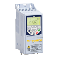
CHAPTER 3 - INSTALLATIONANDCONNECTION
Figure 3.12 b)
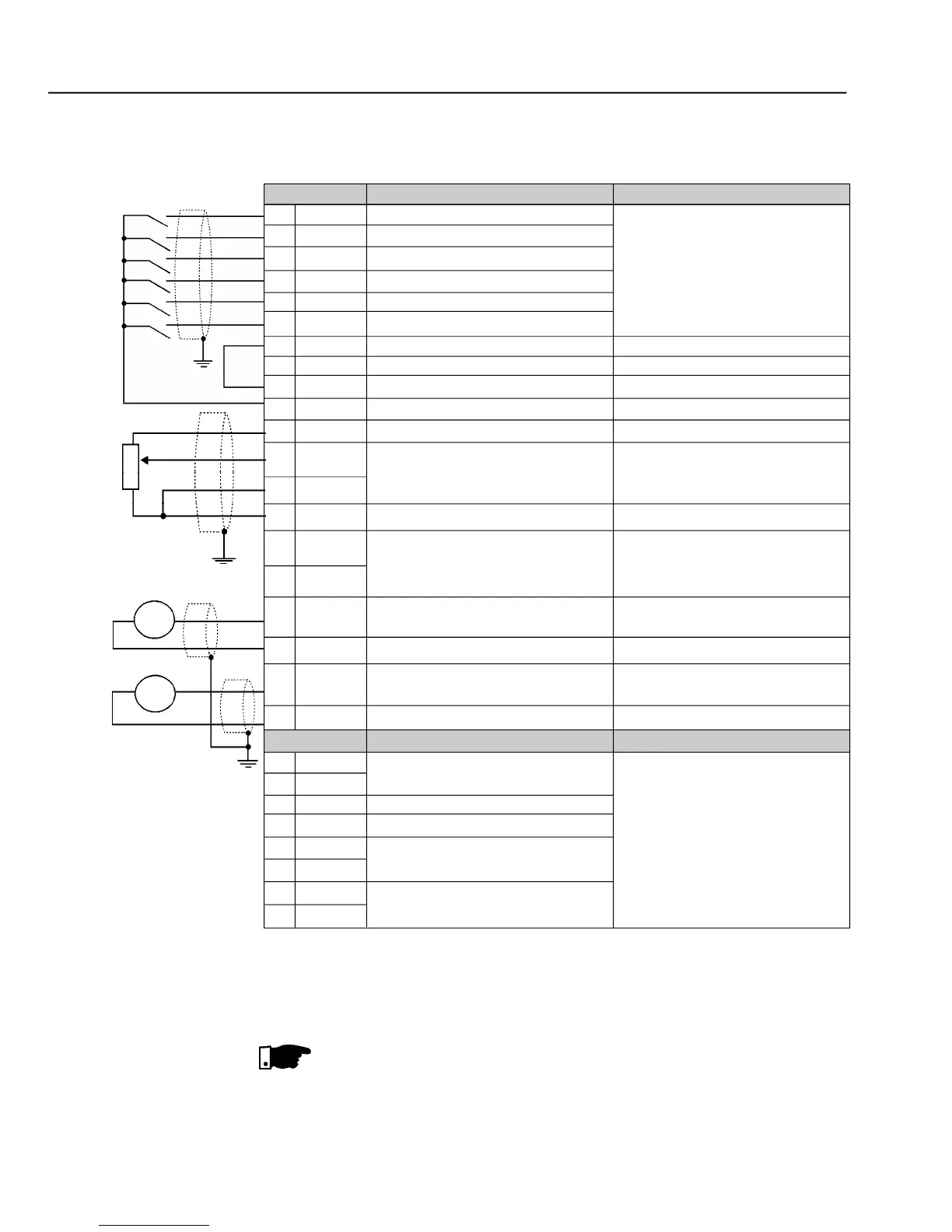
- XC1/XC1A control terminals description (CC9 board) - active low digital inputs
Note:
NC
= normally closed contact,
NO
=
normally open contact,
C
= common
Factory Default Function
Start / Stop
FWD / REV Section (Remote Mode)
No function
No function
JOG (Remote Mode)
Ramp 2 Selection
Digital Inputs Common
Digital inputs 24 Vdc source
0 V Reference of the 24 Vdc Source
Positive Reference for Potentiometer
Analog Input 1:
Speed Reference (Remote Mode)
Negative Reference for Potentiometer
Analog Input 2:
No Function
Analog Output 1: Speed
0 V Reference for Analog Outputs
Analog Output: Motor Current
0 V Reference for Analog Outputs
Factory Default Function
Relay Output - No Fault
Relay Output - Speed > P288 (N > Nx)
Relay Output - No Fault
Relay Output - Speed > P288 (N > Nx)
Relay Output - Speed Reference > P288
(N* > Nx)
Terminal XC1
1
DI1
2
DI2
3
DI3
4
DI4
5
DI5
6
DI6
7
COM
8
COM
9
24 Vdc
10
GND
11
+REF
12
AI1+
13
AI1-
14
-REF
15
AI2+
16
AI2-
17
AO1
18
GND(AO1)
19
AO2
20
GND(AO2)
Terminal
XC1A
21
RL1NC
22
RL1 NO
23
RL2 NO
24
RL1 C
25
RL2 C
26
RL2NC
27
RL3 NO
28
RL3 C
Specifications
6 Isolated Digital Inputs
Minimum High Level: 18 Vdc
Maximum Low Level: 3 Vdc
Maximum Voltage: 30 Vdc
Input Current:
11 mA @ 24 Vdc
Isolated 24 Vdc
±
8 %,Capac: 90 mA
Grounded by a 249 resistor
+ 5.4 Vdc
±
5 %, Capacity: 2 mA
Valid for AI1 and AI2
differential, resolution: (0 to 10) Vdc or
(0 to 20) mA / (4 to 20) mA
-4.7 Vdc
±
5 %, Capacity: 2 mA
Valid for AI1 and AI2
Impedance: 400 k [(0 to 10) Vdc]
500 [(0 to 20) mA / (4 to 20) mA]
(0 to 10) Vdc, R
L
10 k (Max load.)
resolution: 11 bits
Grounded by a 5.1
resistor
(0 to 10) Vdc, R
L
10 k
(Max. Load)
Resolution: 11 bits
Grounded by a 5.1
resistor
Specification
Contact capacity:
1 A
240 Vac
rpm
A
CCW
5 k
CW
The following diagram shows the control wiring with the digitalinputs as active
low(without a jumper betweenXC1:8 and XC1:10).
NOTE!
For using the digitalinputs as active low it is necessary to remove the jumper
between XC1:8 andXC1:10 and place it between XC1:7 and XC1:9.

Table of Contents