3 Wiring and Connection
3.4.2 Output Signal Allocations
3-28
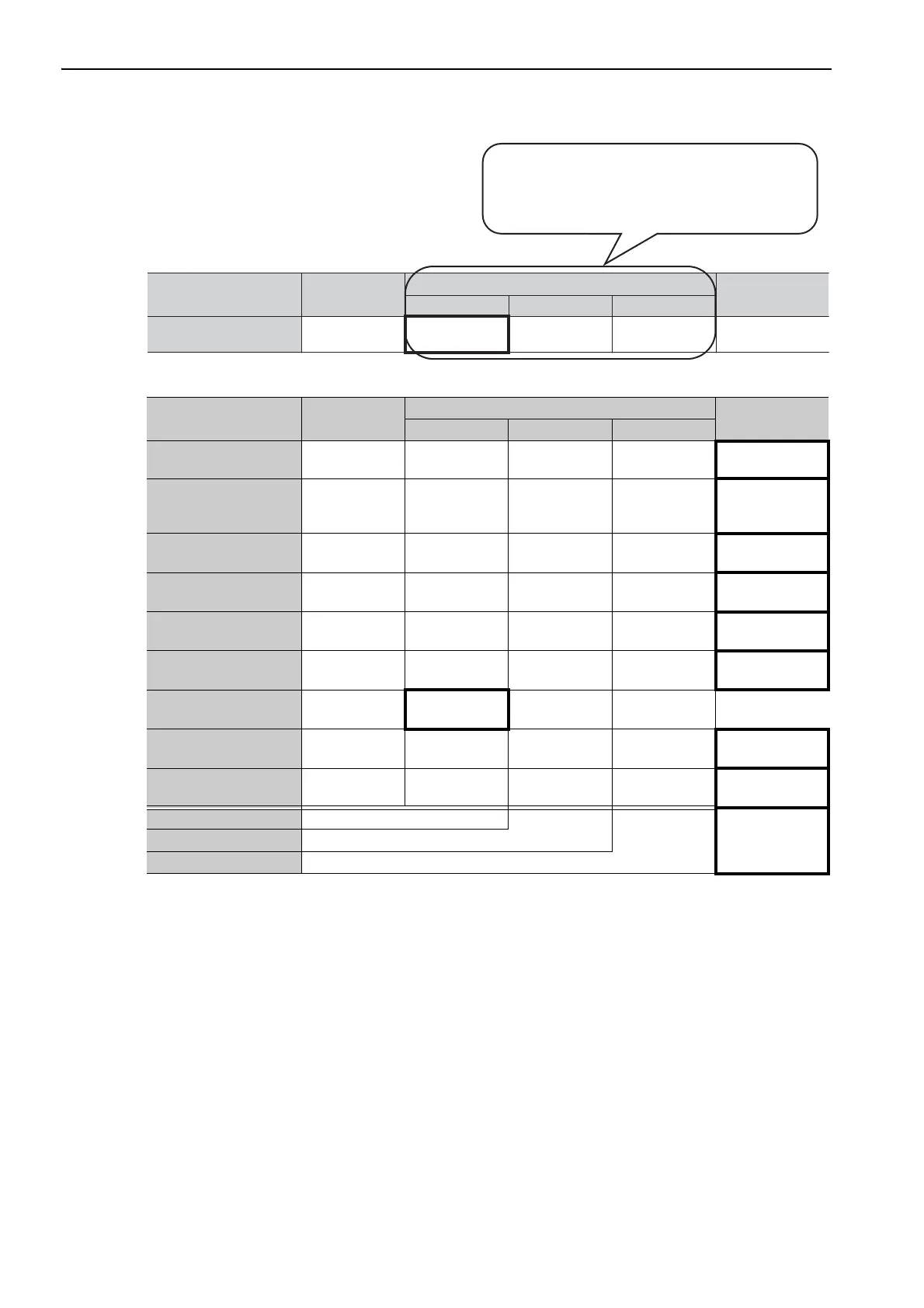
Output Signal Names
and Parameters
Output Signal
CN1 Pin Numbers
Invalid
(not use)
25/ (26) 27/ (28) 29/ (30)
Positioning Completion
Pn50E.0
/COIN 1 2 3 0
Speed Coincidence
Detection
Pn50E.1
/V-CMP 1 2 3 0
Rotation Detection
Pn50E.2
/TGON 1 2 3 0
Servo Ready
Pn50E.3
/S-RDY 1 2 3 0
Torque Limit Detection
Pn50F.0
/CLT 1 2 3 0
Speed Limit Detection
Pn50F.1
/VLT 1 2 3 0
Brake
Pn50F.2
/BK 1 2 3 0
Warning
Pn50F.3
/WARN 1 2 3 0
Near
Pn510.0
/NEAR 1 2 3 0
Pn512.0=1 Polarity inversion of CN1-25(26)
0
(Not invert at
factory setting)
Pn512.1=1 Polarity inversion of CN1-27(28)
Pn512.2=1 Polarity inversion of CN1-29(30)
Output Signal
CN1 Pin Numbers
Invalid
㧔not use㧕
25 (26) 27 (28) 29 (30)
Brake
Pn50F.2
/BK 1 2 3 0
The parameter set values to be used are shown.
Signals are allocated to CN1 pins according to the
selected set values.
Values in cells in bold lines are the factory settings.
Output Signal Names
and Parameters
 Loading...