Titanium Interfaces User Guide
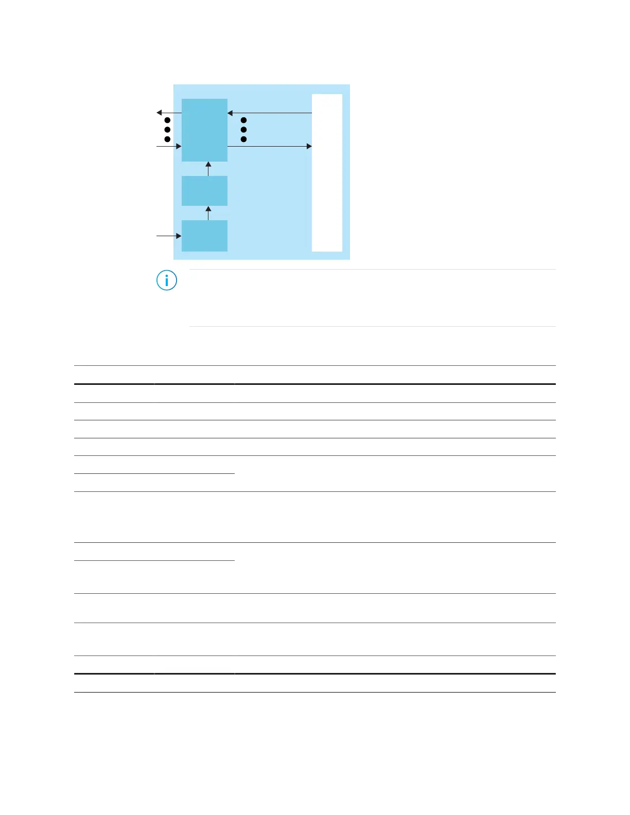
Figure 11: DDR DRAM Interface Block Diagram
Reference Clock
PHY and AXI
Signals
Note: The PLL reference clock must be driven by I/O pads. The Efinity
®
software issues
a warning if you do not connect the reference clock to an I/O pad. (Using the clock tree
may induce additional jitter and degrade the DDR performance.) Refer to About the
PLL Interface on page 121 for more information about the PLL block.
Table 9: DDR DRAM Pads
Signal Direction Description
A[5:0] Output Address signals to the memories.
CS_N[3:0] Output Chip Select to memories.
CKE[1:0] Output Active-high clock enable signals to the memories.
RST_N Output Active-low reset signals to the memories.
CK Output
CK_N Output
Differential active-high clock signals to/from the memories.
DQ[n:0] Bidirectional Data bus to/from the memories. For writes, the pad drives these signals.
For reads, the memory drives these signals. These signals are connected
to the DQ inputs on the memories. n is 15 or 31 depending on the DQ
Width Configuration setting.
DQS_N[n:0] Bidirectional
DQS[n:0] Bidirectional
Differential data strobes to/from the memories. For writes, the pad drives
these signals. For reads, the memory drives these signals. These signals
are connected to the DQS inputs on the memories. n is 1, 1:0, or 3:0
depending on the DQ width.
DM[n] Bidirectional Active-high data-mask signals to the memories. n is 1, 1:0, or 3:0
depending on the DQ width.
Table 10: Calibration Resistor Pad
Signal Direction Description
CAL Input Calibration resistor connection.
www.efinixinc.com 32