Titanium Interfaces User Guide
MIPI TX Lane
In TX mode, a PLL generates the parallel and serial clocks and passes them to the clock and
data lanes.
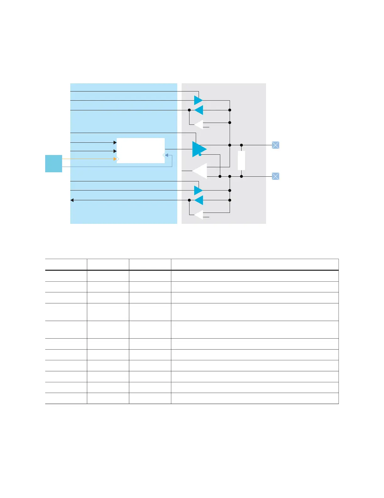
Figure 37: MIPI TX Lane Block Diagram
Table 51: MIPI TX Lane Signals
Interface to MIPI soft CSI/DSI controller with D-PHY in FPGA fabric
Signal Direction Clock Domain Description
HS_OUT[7:0] Input SLOWCLK High-speed output data from the core. Always 8-bits wide.
LP_P_OUT Input – Low-power output data from the core for the P pad.
LP_N_OUT Input – Low-power output data from the core for the N pad.
LP_P_IN Output – (Optional) Low-power input data from the P pad. Used if data
lane is reversible.
LP_N_IN Output – (Optional) Low-power input data from the N pad. Used if data
lane is reversible.
SLOWCLK Input – Parallel (slow) clock.
FASTCLK Input – Serial (fast) clock.
RST Input SLOWCLK (Optional) Resets the serializer.
HS_OE Input – High-speed output enable signal.
LP_P_OE Input – Low-power output enable signal for P pad.
LP_N_OE Input – Low-power output enable signal for N pad.
www.efinixinc.com 98