Here’s an example of usage of these registers on TRK-MPC5604B:
We can notice that use of data input/output registers get repetitive when multiple pads has to be
changed or read. There are parallel input/output registers which simplifies this issue.
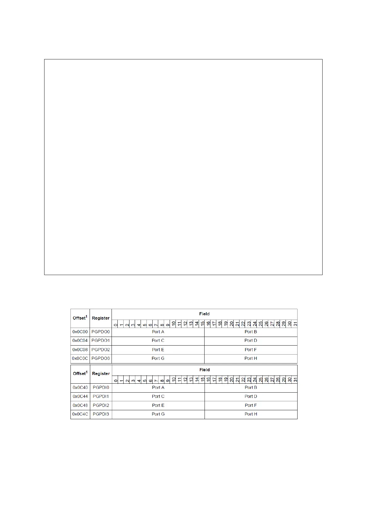
Figure 26 : Parallel GPIO Pad Data In/Out Registers (Reference Manual Rev7 – Table 8-16/17)
These registers allow us to read/write multiple pads on ports with 32 bit registers. For writing
multiple pads masks are often necessary to only change pads of interest, there are masked
parallel registers which simplifies this problem (see figure below).
/* This extract of code will blink LEDs 1 to 4 sequentially while the button S1
is pressed. */
uint32_t LED_state, i;
int main (void) {
initModesAndClock(); /* Initialisation of the device */
config_PORT_E(); /* Configuration of GPIO */
for (; ;) /* Main loop */
{
/* while button is pressed(signal is 0, see schematic) */
for (LED_state=0; !SIU.GPDI[64].B.PDI; LED_state++)
{
if (LED_state==4)
{
LED_state = 0;
SIU.GPDO[68].B.PDO = 1; // All LEDs are off.
SIU.GPDO[69].B.PDO = 1; // -
SIU.GPDO[70].B.PDO = 1; // -
SIU.GPDO[71].B.PDO = 1; // - */
}
SIU.GPDO[68+ LED_state].B.PDO = 0; /* Set next LED */
for (i=0; i<4500000; i++){} /* wait a while */
}
/* while button is not pressed */
for (; SIU.GPDI[64].B.PDI;){}
}
}